GaN-based high-electron-mobility transistor epitaxial wafer and preparation method thereof
A high electron mobility, gallium nitride based technology, applied in the field of gallium nitride based high electron mobility transistor epitaxial wafers and their preparation, can solve high activation energy, large lattice mismatch, poor crystal quality of epitaxial wafers, etc. problem, to achieve the effect of increasing the doping concentration
- Summary
- Abstract
- Description
- Claims
- Application Information
AI Technical Summary
Problems solved by technology
Method used
Image

Examples
Embodiment Construction
[0030] In order to make the purpose, technical solution and advantages of the present disclosure clearer, the implementation manners of the present disclosure will be further described in detail below in conjunction with the accompanying drawings.
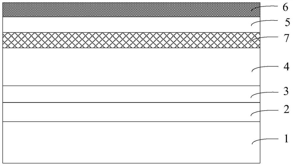
[0031] figure 1 It is a schematic structural diagram of a gallium nitride-based high electron mobility transistor epitaxial wafer provided by an embodiment of the present disclosure, as shown in figure 1 As shown, the gallium nitride-based high electron mobility transistor epitaxial wafer includes a substrate 1 and a buffer layer 2 stacked on the substrate 1, a high-resistance buffer layer 3, a channel layer 4, an AlGaN barrier layer 5 and a cap layer 6.
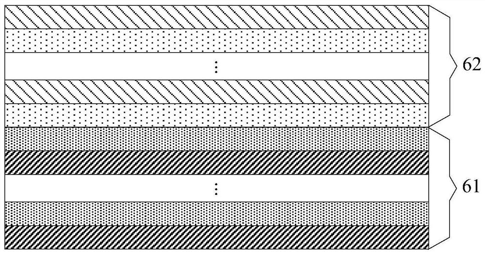
[0032] figure 2 is a schematic structural diagram of a cap layer provided by an embodiment of the present disclosure, such as figure 2 As shown, the capping layer 6 includes a first semiconductor layer 61 and a second semiconductor layer 62 stacked in sequence. The first se...
PUM
| Property | Measurement | Unit |
|---|---|---|
| Thickness | aaaaa | aaaaa |
| Thickness | aaaaa | aaaaa |
| Thickness | aaaaa | aaaaa |
Abstract
Description
Claims
Application Information