Graphene high-sensitivity photoelectric detector and preparation method thereof
A photodetector and high-sensitivity technology, applied in circuits, electrical components, semiconductor devices, etc., can solve the problems of low responsivity, low detection sensitivity, and slow response time of photodetectors, and achieve easy large-area integration and quantum efficiency. High, reliable and long life effect
- Summary
- Abstract
- Description
- Claims
- Application Information
AI Technical Summary
Problems solved by technology
Method used
Image
Examples
preparation example Construction
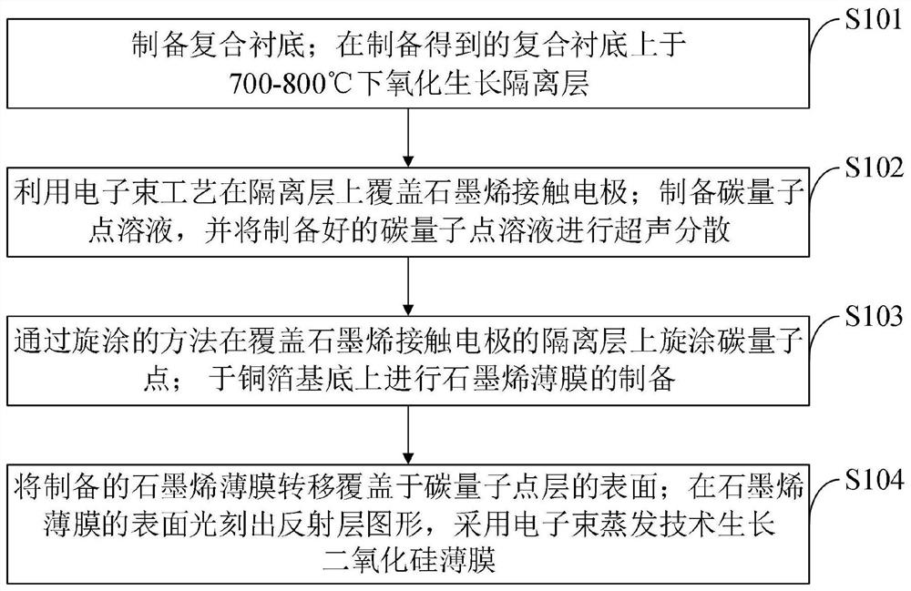
[0052] Such as figure 1 As shown, the preparation method of the graphene high-sensitivity photodetector provided by the embodiment of the present invention comprises the following steps:
[0053] S101, prepare a composite substrate; oxidize and grow an isolation layer at 700-800° C. on the prepared composite substrate;
[0054] S102, using an electron beam process to cover the graphene contact electrode on the isolation layer; preparing a carbon quantum dot solution, and ultrasonically dispersing the prepared carbon quantum dot solution;
[0055] S103, spin-coat carbon quantum dots on the isolation layer covering the graphene contact electrode by spin coating; prepare a graphene film on a copper foil substrate;
[0056] S104, transferring the prepared graphene film to cover the surface of the carbon quantum dot layer; photoetching a reflective layer pattern on the surface of the graphene film, and growing a silicon dioxide film by electron beam evaporation technology.
[005...
Embodiment 1
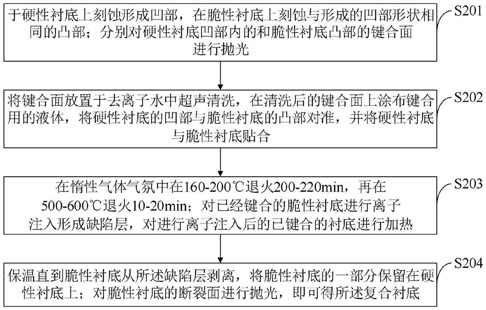
[0062] The preparation method of the graphene high-sensitivity photodetector provided by the embodiment of the present invention is as follows: figure 1 As shown, as a preferred embodiment, such as figure 2 As shown, the preparation method of the composite substrate provided by the embodiment of the present invention includes:
[0063] S201, etching a concave portion on the hard substrate, etching a convex portion with the same shape as the formed concave portion on the brittle substrate; respectively polishing the bonding surfaces of the concave portion of the hard substrate and the convex portion of the brittle substrate;
[0064] S202, place the bonding surface in deionized water for ultrasonic cleaning, apply a bonding liquid on the cleaned bonding surface, align the concave portion of the hard substrate with the convex portion of the brittle substrate, and place the hard substrate Bonding to brittle substrates;
[0065] S203, anneal at 160-200°C for 200-220min in an in...
Embodiment 2
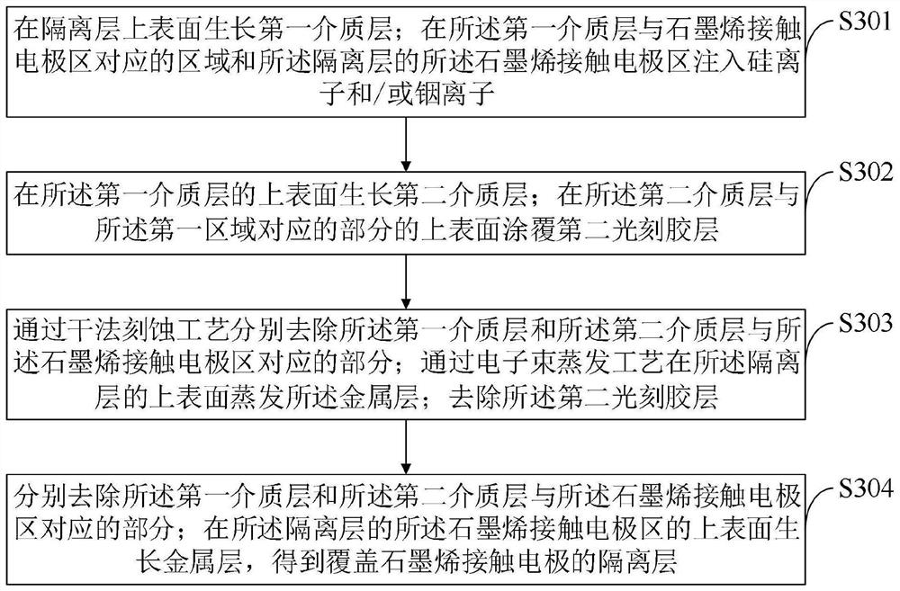
[0070] The preparation method of the graphene high-sensitivity photodetector provided by the embodiment of the present invention is as follows: figure 1 As shown, as a preferred embodiment, such as image 3 As shown, the method for covering the graphene contact electrode on the isolation layer using the electron beam process provided by the embodiment of the present invention includes:
[0071] S301, growing a first dielectric layer on the upper surface of the isolation layer; implanting silicon ions and / or indium ions into the region of the first dielectric layer corresponding to the graphene contact electrode region and the graphene contact electrode region of the isolation layer ;
[0072] S302, growing a second dielectric layer on the upper surface of the first dielectric layer; coating a second photoresist layer on the upper surface of the part of the second dielectric layer corresponding to the first region;
[0073] S303, respectively removing the parts of the first d...
PUM
 Abstract
Description
Claims
Application Information


