
Composite material and preparation method thereof

A composite material and oxide layer technology, which is applied in the manufacture of final products, sustainable manufacturing/processing, electrical components, etc., can solve problems such as poor performance of optoelectronic devices, many surface defects of silicon nanowires, and low luminous efficiency of silicon quantum dots , to achieve the effect of improving the luminous intensity and increasing the probability of

Pending Publication Date: 2021-05-07
TCL CORPORATION
View PDF8 Cites 0 Cited by
  • Summary
  • Abstract
  • Description
  • Claims
  • Application Information

AI Technical Summary

Problems solved by technology

[0006] In view of the above-mentioned deficiencies in the prior art, the object of the present invention is to provide a composite material and a preparation method thereof, aiming at solving the problem that the silicon quantum dots emit light when the composite material formed by the existing silicon quantum dots and silicon nanowires is applied to an optoelectronic device. Low efficiency and many surface defects of silicon nanowires lead to poor performance of optoelectronic devices

Method used

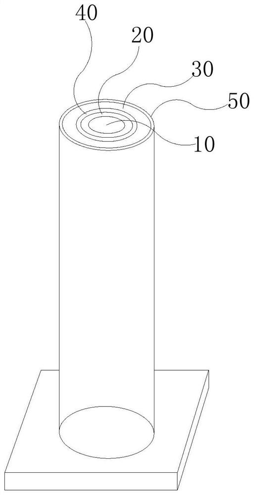
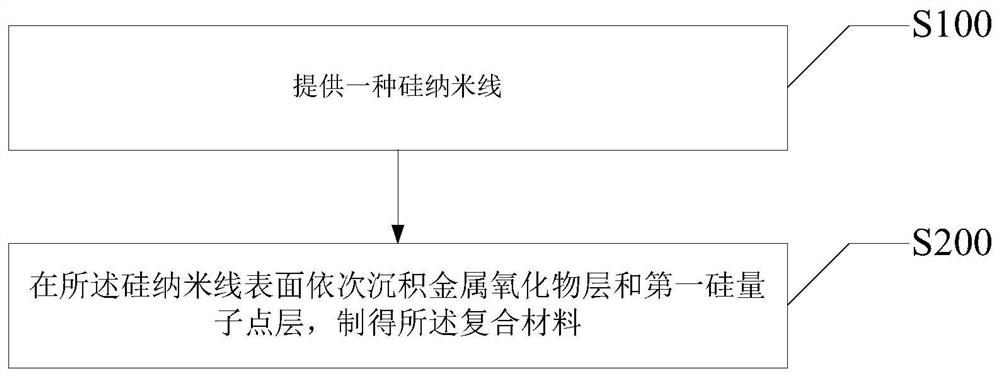

Image

  • Composite material and preparation method thereof
  • Composite material and preparation method thereof

Examples


Embodiment approach

[0038] Some embodiments of the present invention, the preparation of described composite material also comprises the step:

[0039] Alternating layers are deposited on the surface of the first silicon dioxide layer, and the alternating layers include second silicon quantum dot layers and second silicon dioxide layers alternately in sequence.

[0040] In some embodiments, the step of preparing the alternating layers comprises:

[0041] In the first step, 5-10% SiH is introduced into the reaction chamber 4 Gas and 90-95% Ar gas are used as reaction gases, and the flow rate is controlled at 5-15 standard ml / min by adjusting the mass flow meter; after the gas flow is stable, turn on the RF plasma power supply, the RF power is 50-60W, and the temperature Keep the temperature at 200-260°C for plasma chemical vapor deposition to prepare a silicon film, and deposit for 10-15s;

[0042] In the second step, continue to feed oxygen into the reaction chamber as the reaction gas, and con...

Embodiment 1

[0047] Preparation of silicon nanowires:

[0048] Mix silver nitrate, hydrofluoric acid and deionized silicon according to the mass ratio of 1:2:6 to prepare an etching solution; then place the silicon wafer in the etching solution for 10 minutes, take it out and wash it with concentrated nitric acid Wash with deionized water several times to obtain silicon nanowires.

[0049] The preparation of composite material, specific steps are as follows:

[0050] Using gaseous trimethylaluminum as the precursor, water as the reactant and nitrogen as the carrier gas, set the temperature of the reaction chamber at 160°C, the process pressure at 0.2torr, and the cycle period of 50 to prepare a 4nm-thick aluminum oxide film on the surface of the silicon nanowire . Put the above-mentioned silicon nanowires deposited with alumina into a vacuum chamber, and nitrogen gas is introduced after vacuuming, the total sputtering pressure is at 1Pa, and then a nano-metal layer is deposited on the su...

Embodiment 2

[0054] Preparation of silicon nanowires:

[0055] Mix silver nitrate, hydrofluoric acid and deionized silicon according to the mass ratio of 1:2:6 to prepare an etching solution; then place the silicon wafer in the etching solution for 10 minutes, take it out and wash it with concentrated nitric acid Wash with deionized water several times to obtain silicon nanowires.

[0056] The preparation of composite material, specific steps are as follows:

[0057] Using gaseous trimethylaluminum as the precursor, water as the reactant and nitrogen as the carrier gas, set the temperature of the reaction chamber at 160°C, the process pressure at 0.2torr, and the cycle period of 50 to prepare a 4nm-thick aluminum oxide film on the surface of the silicon nanowire . Put the above-mentioned silicon nanowires deposited with alumina into a vacuum chamber, and nitrogen gas is introduced after vacuuming, the total sputtering pressure is at 1Pa, and then a thin layer of gold is deposited on the ...


PUM

PropertyMeasurementUnit
thicknessaaaaaaaaaa
thicknessaaaaaaaaaa
thicknessaaaaaaaaaa

Abstract

The invention discloses a composite material and a preparation method thereof. The composite material comprises a silicon nanowire, a metal oxide layer and a first silicon quantum dot layer, wherein the surface of the silicon nanowire is coated with the metal oxide layer, and the surface of the metal oxide layer is coated with the first silicon quantum dot layer. According to the invention, the metal oxide layer can effectively passivate interface defects between the silicon nanowires and the first silicon quantum dot layer and dangling bonds on the surfaces of the first silicon quantum dots, so electrons are prevented from being quenched due to non-radiative recombination at the interface defects and on the surfaces of the first silicon quantum dots; besides, due to the electronegativity of the metal oxide, a local electrostatic field can be formed in the space around the metal oxide, and injected electrons are prevented from being directly captured by silicon nanowire defects; meanwhile, positive electrode holes are attracted to be injected into the first silicon quantum dot layer, and therefore, the probability of combination of the electrons and the holes is increased, the luminous intensity of the first silicon quantum dot layer is improved, so that the electroluminescent performance of the composite material is improved.

Description

technical field [0001] The invention relates to the field of silicon quantum dots, in particular to a composite material and a preparation method thereof. Background technique [0002] As a very common element, silicon rarely occurs in nature in the form of simple substance, and it usually exists widely in rocks, gravel and dust in the form of supported silicate or silicon dioxide. Silicon is a semiconductor material that can be used to make semiconductor devices, solar panels, and integrated circuits. It can also be used in automotive and mechanical parts in the form of alloys, and can also be used in cermets together with ceramic materials. In addition, silicon can also be used in the manufacture of glass, concrete, bricks and refractory materials. [0003] Silicon quantum dots generally refer to silicon nanocrystals with a size not greater than 10nm. Due to the quantum confinement effect, electrons and holes in silicon quantum dots may recombine without the participation...

Claims


Application Information

Patent Timeline
Patent Type & Authority Applications(China)
IPC IPC(8): H01L31/0352H01L31/18
CPCH01L31/035227H01L31/035254H01L31/1804Y02P70/50
Inventor 叶炜浩邹文鑫
Owner TCL CORPORATION
Learn More