Homojunction photoelectric detector based on gallium oxide energy band regulation and preparation method thereof

A photodetector, gallium oxide technology, applied in photovoltaic power generation, circuits, electrical components, etc.

Active Publication Date: 2021-06-11
ZHENGZHOU UNIV
View PDF6 Cites 1 Cited by
  • Summary
  • Abstract
  • Description
  • Claims
  • Application Information

AI Technical Summary

Problems solved by technology

[0003]The purpose of the present invention is to solve the problem that Ga2O3 cannot achieve a stable p-type doping-limited homojunction For the preparation of photodetectors, a method was proposed to change the band gap of gallium oxide by adjusting the amount of oxygen in the growth process, and two kinds of gallium oxide with different band gaps were used to prepare homojunction photodetectors

Method used


Image

  • Homojunction photoelectric detector based on gallium oxide energy band regulation and preparation method thereof
  • Homojunction photoelectric detector based on gallium oxide energy band regulation and preparation method thereof
  • Homojunction photoelectric detector based on gallium oxide energy band regulation and preparation method thereof

Examples


preparation example Construction

[0043] The preparation method of the homojunction photodetector based on gallium oxide energy band regulation comprises the following steps:

[0044] (1) cleaning the substrate;

[0045] (2) Depositing amorphous Ga on the substrate by plasma-enhanced chemical vapor deposition 2 o 3 film;

[0046] (3) In the amorphous Ga 2 o 3 Deposit β-phase Ga on the thin film using plasma enhanced chemical vapor deposition technology 2 o 3 film;

[0047] (4) Magnetron sputtering technology was used to separate two Ga 2 o 3 Sputtering titanium gold electrodes on the film;

[0048] (5) Using high-temperature annealing technology, the two electrodes are separated from the amorphous Ga 2 o 3 and β-Ga 2 o 3 form an ohmic contact.

[0049] The gallium source used in plasma enhanced chemical vapor deposition in step (2) is triethylgallium, the gas required for growth is nitrogen and oxygen, the gas flow rate is 15 and 3-8 sccm respectively, and the growth temperature is 400-600 ° C. ...

Embodiment 1

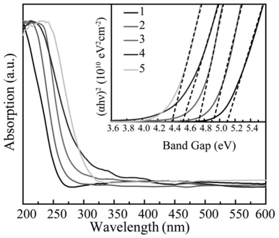
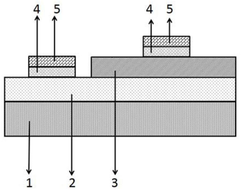
[0054] In steps (2) and (3), during the preparation of gallium oxide, amorphous Ga is grown by controlling the amount of oxygen and nitrogen. 2 o 3 Thin film and β-phase Ga 2 o 3 The bandgap and conductivity of the film. After two gallium oxide films with different bandgaps are in contact, due to the difference in Fermi level, a built-in electric field is formed at the interface. The energy band diagram is shown in Figure 4.

[0055] In this instance, in step (2), amorphous Ga 2 o 3 In the process of film preparation, the nitrogen and oxygen flow rates were 15 and 5 sccm respectively, the growth temperature was 500°C, the growth time was 1.5 hours, and the growth thickness was about 100 nanometers. In step (3), the β-phase Ga 2 o 3 During the film preparation process, the nitrogen and oxygen gas flow rates were 15 and 15 sccm, the growth temperature was 500 degrees, the growth time was 1.0 hour, and the growth thickness was about 45 nanometers. The amorphous Ga 2 o 3 Th...

Embodiment 2

[0058] This example is different from Example 1, changing the ratio of nitrogen and oxygen in the process of growing gallium oxide twice, growing amorphous Ga in this example 2 o 3 Thin film and β-phase Ga 2 o 3 During the thin film process, the nitrogen and oxygen gas flow rates were 15, 3sccm and 15, 20sccm respectively, and the band gaps were 4.1 and 5.1eV respectively. According to the above device preparation process, the following figure 1 For the homojunction photodetector shown, the device is annealed in a high-temperature tube furnace after preparation, and the annealing temperature and time are 400° C. and 10 minutes, respectively. By carrying out the spectral response test under zero volt bias, the response curve is as follows Figure 7 shown. From Figure 7 It can be seen that the response spectrum in the deep ultraviolet region is significantly larger than that in the visible region, which indicates that the photodetector also has a photovoltaic effect in thi...


PUM

PropertyMeasurementUnit
electrical resistivityaaaaaaaaaa
thicknessaaaaaaaaaa
electrical resistivityaaaaaaaaaa

Abstract

The invention provides a gallium oxide energy band regulation-based homojunction photoelectric detector and a preparation method thereof. The homojunction photoelectric detector comprises an insulated substrate, the substrate (1) is sequentially provided with an amorphous Ga2O3 film and a beta-phase Ga2O3 film, and the amorphous Ga2O3 film and the beta-phase Ga2O3 film are both provided with contact electrodes. Aiming at the problem that Ga2O3 cannot realize stable p-type doping to limit the preparation of the homojunction photoelectric detector, the invention provides a method for preparing the homojunction photoelectric detector by regulating and controlling the amount of oxygen in the growth process to change the gallium oxide band gap and utilizing the gallium oxide with two different band gaps, so the problem of p-type doping of Ga2O3 during the preparation of the homojunction photoelectric detector is solved; and a foundation is laid for energy band regulation and control of Ga2O3 and preparation and research of a high-performance Ga2O3 homojunction photoelectric detector.

Description

technical field [0001] The invention relates to the field of photoelectric device preparation, in particular to a homojunction photodetector based on gallium oxide energy band regulation and a preparation method thereof. Background technique [0002] Gallium oxide (Ga 2 o 3 ) as an ultra-wide bandgap semiconductor, due to its high breakdown field, high thermal and chemical stability, and high Ballyga figure of merit, it has attracted great attention in the fields of power electronics, solar-blind photodetectors and sensors. extensive attention. In addition, for Ga prepared under different conditions 2 o 3 The samples were studied and found that their bandgap varied between 4.4-5.1eV, corresponding to wavelengths of 234-280nm in the solar-blind region, making them suitable for solar-blind light detection. Various Ga-based 2 o 3 electronic and optoelectronic devices, however, how to improve Ga-based 2 o 3 The performance of devices is one of the most challenging issue...

Claims


Application Information

Patent Timeline
Patent Type & Authority Applications(China)
IPC IPC(8): H01L31/18H01L31/068H01L31/032C23C14/18C23C14/35C23C14/58C23C16/40C23C16/50C23C28/00
CPCH01L31/068H01L31/18H01L31/032C23C16/50C23C16/40C23C14/35C23C14/5806C23C14/185C23C28/345C23C28/321Y02E10/547Y02P70/50
Inventor 杨珣陈彦成单崇新
Owner ZHENGZHOU UNIV
Why Eureka
Try Eureka