Method for realizing positive and negative photoconduction in memristor by using optical signal

A photoconductive and optical signal technology, applied in electrical components and other directions, can solve problems such as no literature reports, and achieve the effects of simple and effective method, simple preparation, and broad application prospects.

Active Publication Date: 2021-06-11
NINGBO INST OF MATERIALS TECH & ENG CHINESE ACADEMY OF SCI
View PDF5 Cites 1 Cited by
  • Summary
  • Abstract
  • Description
  • Claims
  • Application Information

AI Technical Summary

Problems solved by technology

So far, there is no literature report to achieve positive and negati

Method used


Image

  • Method for realizing positive and negative photoconduction in memristor by using optical signal
  • Method for realizing positive and negative photoconduction in memristor by using optical signal
  • Method for realizing positive and negative photoconduction in memristor by using optical signal

Examples


Embodiment 1

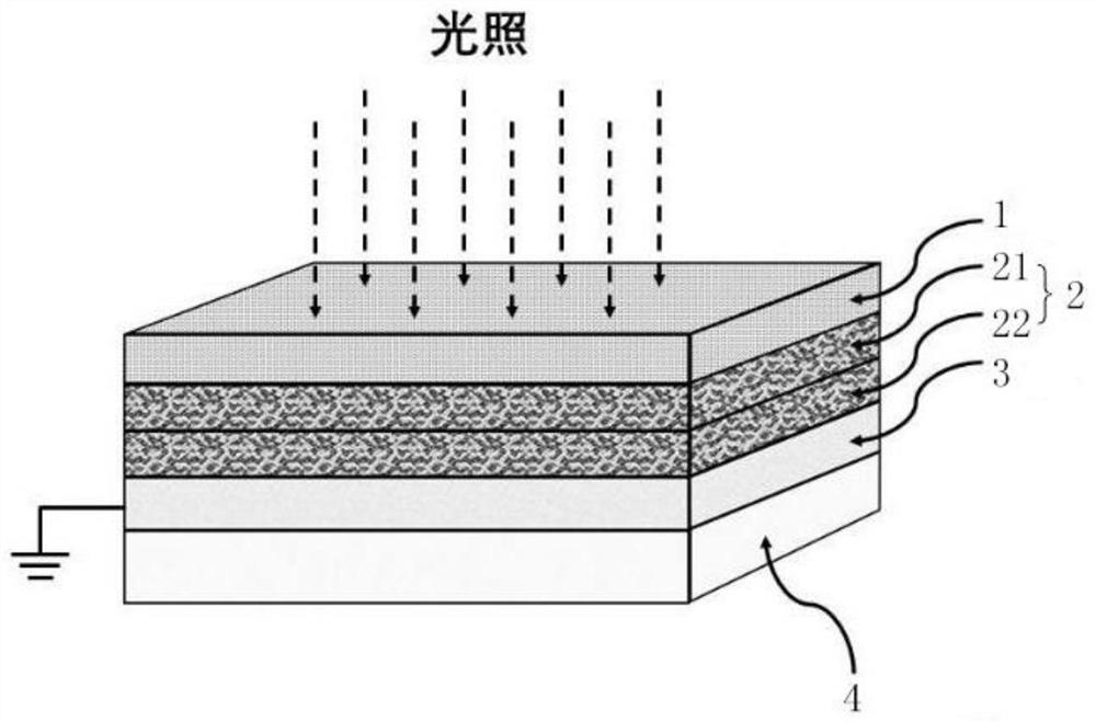
[0047] A memristor, comprising sequentially forming a bottom electrode layer 3 , an oxide layer 2 (an oxygen-deficient layer 22 and an oxygen-rich layer 21 ) and a top electrode layer 1 on a substrate 4 . The substrate in this embodiment is a thermally oxidized silicon wafer, the material of the bottom electrode layer 3 is platinum, and its thickness is 150 nm; the material of the oxide layer 2 is indium gallium zinc oxide (IGZO), which includes an oxygen-deficient layer and an oxygen-rich layer, and The thickness of the oxygen layer is 60nm, and the thickness of the oxygen-enriched layer is 20nm; the material of the top electrode layer is gold, and its thickness is 10nm.

[0048] The preparation method of the memristor of the present embodiment is as follows:

[0049] (1) A 6nm-thick titanium film was prepared on the surface of the substrate by electron beam evaporation as a buffer layer. The main function was to increase the mechanical bonding force between the platinum film...

Embodiment 2

[0060] The difference from Example 1 is that the bottom electrode layer is tin-doped indium oxide (ITO) grown by magnetron sputtering, with ITO as the sputtering target, with argon as the sputtering atmosphere, the substrate temperature is room temperature, and the sputtering The power is 20-100W, the temperature is 20-50°C, and the time is 1-120min. The thickness of the ITO film is 200nm, the IGZO film includes an oxygen-deficient layer and an oxygen-rich layer, the thickness of the oxygen-deficient layer is 60nm, the thickness of the oxygen-rich layer is 20nm, and the thickness of the gold electrode is 10nm.

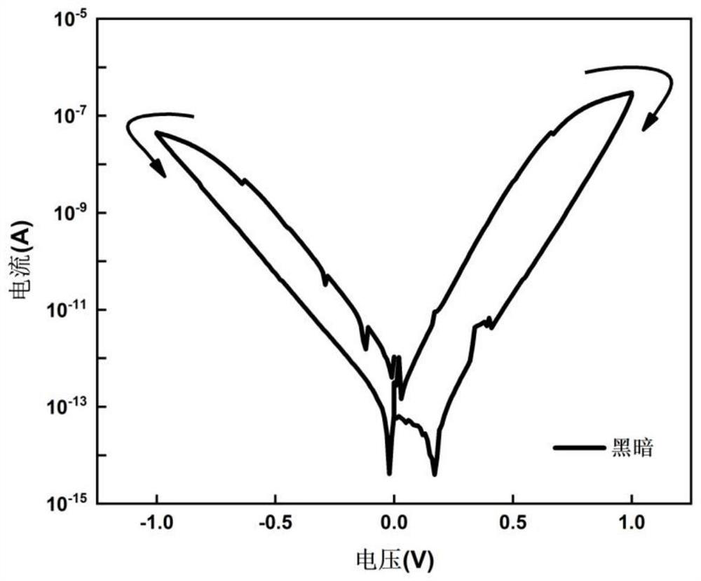
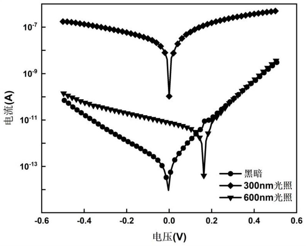
[0061] Figure 6 The current-voltage characteristic curve of the memristor prepared for this example in a dark environment, the bottom electrode is grounded, and the voltage is applied to the top electrode, and an obvious hysteresis window can be seen. Figure 7The current-voltage linear scanning curve of the memristor prepared for this example under a dark environmen...


PUM

PropertyMeasurementUnit
Thicknessaaaaaaaaaa
Thicknessaaaaaaaaaa
Thicknessaaaaaaaaaa

Abstract

The invention discloses a method for realizing positive and negative photoconduction in a memristor by using an optical signal. The memristor comprises a bottom electrode layer, a top electrode layer and an oxide layer located between the bottom electrode layer and the top electrode layer, wherein the oxide layer comprises an oxygen-enriched layer and an oxygen-deficient layer, the oxygen-enriched layer is adjacent to the top electrode layer, and the oxygen-deficient layer is adjacent to the bottom electrode layer. According to the method, the optical signal is input through the top electrode layer, and the method comprises the steps that the memristor obtains a positive photoconduction mode or a negative photoconduction mode through the optical signal; in the forward photoconduction mode, the optical signal is ultraviolet light; and in the negative photoconduction mode, the optical signal is visible light or infrared light. By utilizing the own characteristics of the memristor disclosed by the invention, the reversible regulation and control of the positive and negative conductance polarities of the memristor can be realized under the optical signals with different wavelengths.

Description

technical field [0001] The invention relates to the field of optoelectronic technology, more specifically, to a method for regulating the positive and negative polarities of a memristor photoconductor by using an optical signal. Background technique [0002] With the advent of the era of artificial intelligence and big data, the requirements for real-time information transmission and processing on computer performance continue to increase. In the traditional Von Neumann computer architecture, the computing power improvement scheme based on Moore's Law has gradually been limited by physical bottlenecks, and scaling and integration of devices can no longer provide the required performance gain. The human brain can store and process information in parallel and perform large-scale calculations, which greatly reduces power consumption. The development of brain-like smart devices is one of the important directions to break through the current technological bottleneck. [0003] Me...

Claims


Application Information

Patent Timeline
IPC IPC(8): H01L45/00
CPCH10N70/801H10N70/821H10N70/8836H10N70/026
Inventor 诸葛飞沈柳枫胡令祥张莉
Owner NINGBO INST OF MATERIALS TECH & ENG CHINESE ACADEMY OF SCI
Why Eureka
Try Eureka