Passivation process method for gallium nitride and gallium nitride ternary alloy

A gallium nitride III technology, which is applied in electrical components, sustainable manufacturing/processing, climate sustainability, etc., can solve problems such as many surface defects and large leakage current, and achieve improved device performance and operability. Strong, simple effect of passivation process

Inactive Publication Date: 2021-06-29
SHANGHAI INST OF TECHNICAL PHYSICS - CHINESE ACAD OF SCI
View PDF4 Cites 0 Cited by
  • Summary
  • Abstract
  • Description
  • Claims
  • Application Information

AI Technical Summary

Problems solved by technology

[0003] The present invention provides a simple and effective passivation process for gallium nitride and gallium nitride ternary alloys for the problems of too many surface defects and excessive leakage current of gallium nitride and gallium nitride ternary alloy devices

Method used


Image

  • Passivation process method for gallium nitride and gallium nitride ternary alloy
  • Passivation process method for gallium nitride and gallium nitride ternary alloy
  • Passivation process method for gallium nitride and gallium nitride ternary alloy

Examples


Embodiment 1

[0018] Using the present invention to passivate the silicon substrate PIN structure indium gallium nitride ultraviolet detector, the specific process steps are as follows:

[0019] (1) Epitaxially grow buffer layer, n-type gallium nitride, i-type indium gallium nitride, and p-type gallium nitride sequentially on the silicon substrate;

[0020] (2) Perform photolithography on the device to form a mesa structure, and grow p-electrodes and n-electrodes;

[0021] (3) Preferably, the device is immersed in passivation solution A or passivation solution B for passivation, passivation solution A is a mixed solution of ruthenium chloride of 0.01mol / L and nitric acid of 0.1g / L, passivation Solution B is a mixed solution of 0.01mol / L sodium sulfide and 0.1g / L nitric acid, the passivation temperature is 20°C, and the passivation time is 10min. After taking it out, wash it with deionized water and dry it with nitrogen;

[0022] (4) Preferably, a passivation layer of silicon dioxide or sil...

Embodiment 2

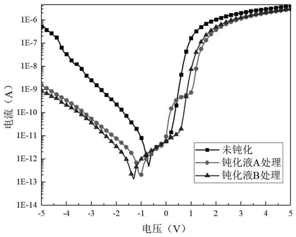
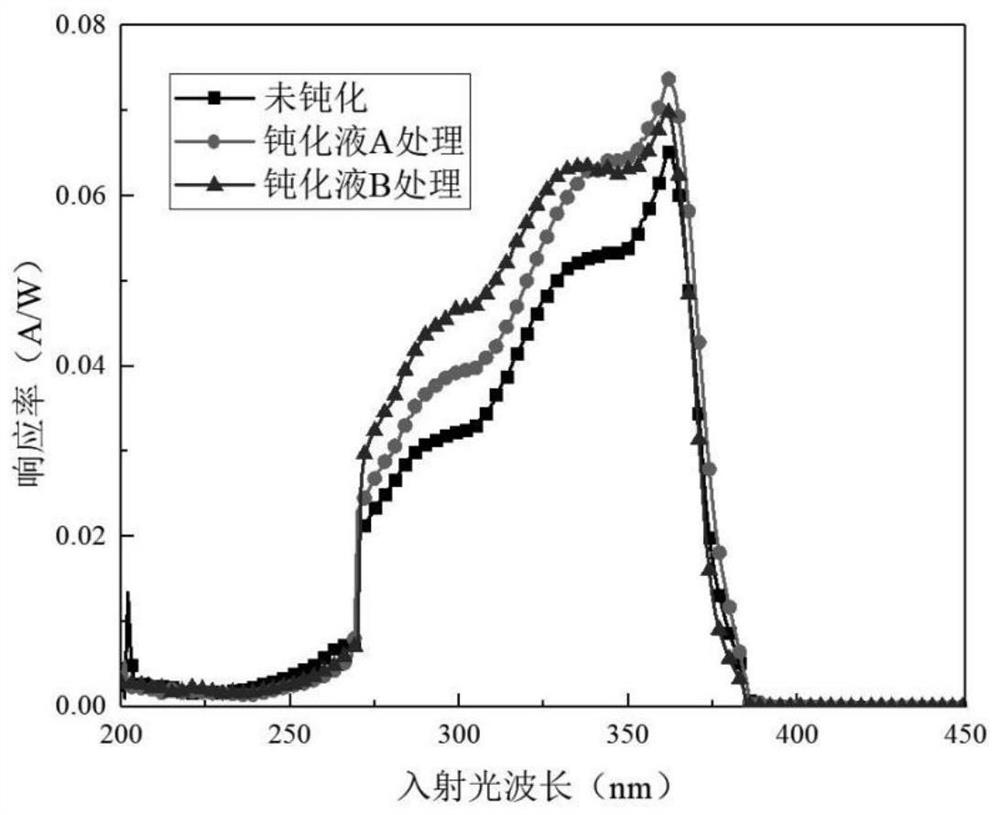
[0026] The specific process steps of this embodiment are similar to those of Embodiment 1, but the passivation temperature in step (3) and step (5) is adjusted to 30°C.

[0027] image 3 is the volt-ampere characteristic curve of the device under different passivation conditions. Compared with the devices without solution passivation, the reverse dark current of the devices treated with passivation solution A and passivation solution B decreased by 2-4 orders of magnitude. Figure 4 is the spectral responsivity curve of the device under different passivation conditions. Compared with the devices without solution passivation, the responsivity of the devices treated with passivation solution A and passivation solution B was significantly improved, and the peak responsivity increased by 15% and 25%, respectively.

Embodiment 3

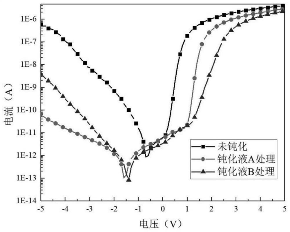
[0029] The specific process steps of this embodiment are similar to those of Embodiment 1, but the passivation temperature in step (3) and step (5) is adjusted to 40°C.

[0030] Figure 5 is the volt-ampere characteristic curve of the device under different passivation conditions. Compared with the devices without solution passivation, the reverse dark current of the devices treated with passivation solution A and passivation solution B decreased by 1-2 orders of magnitude. Figure 6 is the spectral responsivity curve of the device under different passivation conditions. Compared with the device without solution passivation, the responsivity of the device treated with passivation solution A and passivation solution B was significantly improved, and the peak responsivity increased by 1% and 10%, respectively.


PUM

PropertyMeasurementUnit
thicknessaaaaaaaaaa

Abstract

The invention discloses a passivation process method for gallium nitride and gallium nitride ternary alloy. The process method comprises the following steps: carrying out primary passivation on clean gallium nitride and gallium nitride ternary alloy by taking nitric acid, ruthenium trichloride or sodium sulfide as a passivation solution; after first passivation cleaning, epitaxially growing a silicon dioxide or silicon nitride film for second passivation; and after the device is formed, carrying out third passivation by taking nitric acid, ruthenium trichloride or sodium sulfide as a passivation solution. By using the passivation process provided by the invention, a surface leakage current and a dark current of gallium nitride and gallium nitride ternary alloy device are effectively reduced, and the performance of the device is improved.

Description

technical field [0001] The invention relates to the technical field of surface passivation of gallium nitride and gallium nitride ternary alloys, in particular to a passivation process method of gallium nitride and gallium nitride ternary alloys. Background technique [0002] Gallium nitride has a large band gap, high thermal conductivity, and strong radiation resistance. It is widely used in power devices, light-emitting diodes, photoelectric detection and other fields. There is a large lattice mismatch and thermal mismatch between gallium nitride and gallium nitride ternary alloys such as indium gallium nitride, aluminum gallium nitride, etc., and epitaxial substrates such as sapphire, silicon, etc., resulting in epitaxial growth on these substrates. Gallium nitride and gallium nitride ternary alloy thin films have many defects and poor crystal quality, resulting in large surface leakage current and dark current of the device, and poor device performance. Most of the exis...

Claims


Application Information

Patent Timeline
Patent Type & Authority Applications(China)
IPC IPC(8): H01L31/18H01L33/00
CPCH01L31/1868H01L31/184H01L33/005Y02P70/50
Inventor 李浩杰刘向阳张燕王玲许金通李向阳
Owner SHANGHAI INST OF TECHNICAL PHYSICS - CHINESE ACAD OF SCI
Why Eureka
Try Eureka