Light-emitting diode and its preparation method
A technology of light-emitting diodes and light-emitting layers, which is applied in the manufacture of semiconductor/solid-state devices, semiconductor devices, electrical components, etc., can solve the problems of unbalanced electron transfer rate and hole transfer rate, etc., to increase the plasmon resonance effect, improve efficiency, Effect of increasing luminous efficiency and luminous intensity
- Summary
- Abstract
- Description
- Claims
- Application Information
AI Technical Summary
Problems solved by technology
Method used
Image
Examples
Embodiment approach
[0034] As an embodiment, the particle size of the noble metal nanoparticles is 30-50 nanometers.
[0035]In the embodiment of the present invention, the precious metal nanoparticles can be selected from commercially available commodities, and can also be selected from products prepared by conventional technical means in the art.
[0036] In some embodiments, the precious metal nanoparticles are gold nanoparticles, and the preparation method includes:
[0037] (1) In the glassware after washing, rinsing and drying with aqua regia, first add 100 mL of pure water, and then add 1 mL of 0.5 mmol / mL trisodium citrate solution;
[0038] (2) 20mL, 0.0025mmol / mL HAuCl 4 and 10mL, 0.01mmol / ml CTAB (hexadecyltrimethylammonium bromide) mixed solution was rapidly injected into the trisodium citrate solution, vigorously stirred for 1min, and stood still at room temperature for 1h to obtain a precious metal seed solution;
[0039] (3) adding 5mL, 0.01mmol / ml CTAB, 5.5mL, 0.01mmol / ml chloro...
Embodiment 1
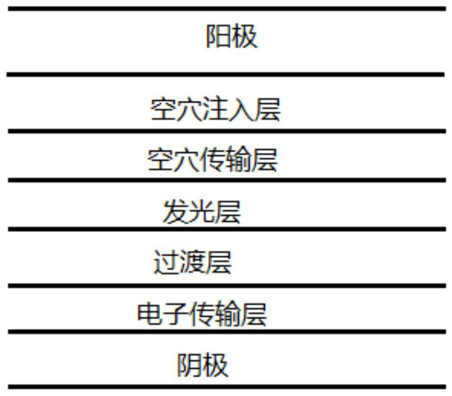
[0070] In this example, a light-emitting diode is prepared, which includes an ITO bottom electrode, a hole injection layer, a hole transport layer, a quantum dot light-emitting layer, a transition layer, an electron transport layer and a cathode that are stacked in sequence.
[0071] The method for preparing the above light-emitting diode specifically includes the following steps:
[0072] 1. Preparation of transition layer material
[0073](1) In the glassware after washing, rinsing and drying with aqua regia, first add 100 mL of pure water, and then add 1 mL of 0.5 mmol / mL trisodium citrate solution;
[0074] (2) 20mL, 0.0025mmol / mL HAuCl 4 and 10mL, 0.01mmol / ml CTAB (hexadecyltrimethylammonium bromide) mixed solution was rapidly injected into the trisodium citrate solution, vigorously stirred for 1min, and stood still at room temperature for 1h to obtain a precious metal seed solution;
[0075] (3) adding 5mL, 0.01mmol / ml CTAB, 5.5mL, 0.01mmol / ml chloroauric acid, 3mL, 0....
Embodiment 2
[0086] In this example, a light-emitting diode is prepared, which is different from Example 1 in that the thickness of the hole injection layer is 25 nanometers; the thickness of the cathode is 10 nanometers.
PUM
| Property | Measurement | Unit |
|---|---|---|
| particle diameter | aaaaa | aaaaa |
| thickness | aaaaa | aaaaa |
| thickness | aaaaa | aaaaa |
Abstract
Description
Claims
Application Information


