

A method and device for wireless photoelectrochemical mechanical polishing of semiconductor wafers
A photoelectrochemical and mechanical polishing technology, which is applied in semiconductor/solid-state device manufacturing, grinding devices, circuits, etc., can solve problems such as inability to process, inability to directly connect to photoelectrochemical systems, etc.
- Summary
- Abstract
- Description
- Claims
- Application Information
AI Technical Summary
Problems solved by technology
Method used
Image

Examples
Embodiment 1
[0045] Embodiment 1 Semiconductor wafer wireless photoelectrochemical mechanical polishing device
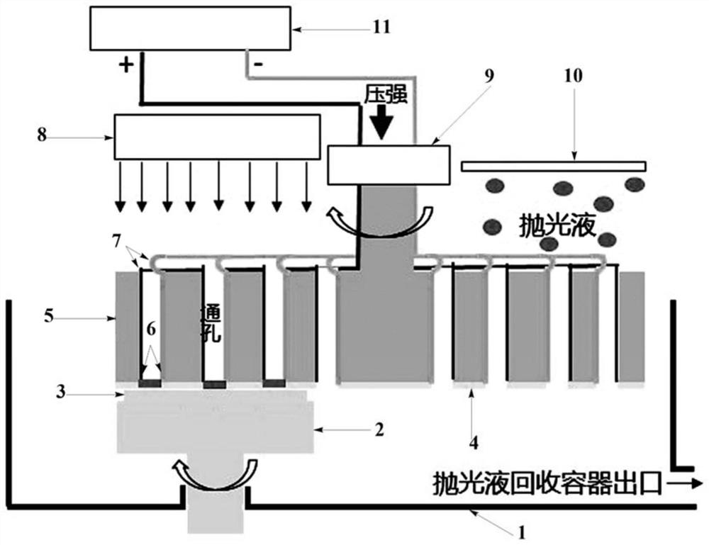
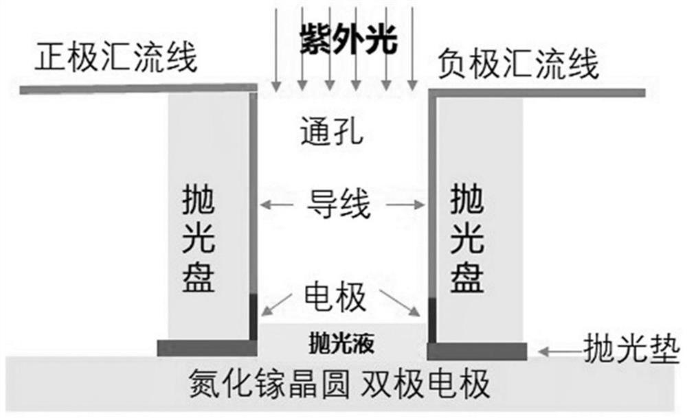
[0046] figure 1 A schematic diagram of a wireless photoelectrochemical mechanical polishing device for semiconductor wafers provided by the present invention: comprising a polishing head (2), a semiconductor wafer (3), a polishing pad (4), a polishing disc (5), and a polishing liquid nozzle (10) , conductive slip ring (9), positive and negative electrode bus wires (7), ultraviolet light source (8), DC power supply (11) and polishing liquid recovery tank (1); wherein, the polishing pad and the polishing disc have the same The through holes arranged in a honeycomb array; the polishing pad is pasted on the bottom of the polishing disc; a pair of positive and negative electrodes (6) are arranged on each through hole bottom wall of the polishing disc, and the positive and negative electrodes Incorporate the positive and negative electrode bus lines arranged on the top of the polishi...
Embodiment 2
[0062] Use the wireless photoelectrochemical mechanical polishing device for semiconductor wafers described in Example 1 to process semiconductor wafers, wherein a polishing disc (2.2 cm in thickness) and a polishing pad (SUBA800) with a diameter of 23 cm are selected according to the Fibonacci array Arrange 131 through holes with a diameter of 0.6 cm; the structure of the photoelectrochemical electrolytic cell used is consistent with the description in the examples. The specific steps of the method for wireless photoelectrochemical mechanical polishing of semiconductor wafers are as follows: the non-intentionally doped n-type gallium nitride wafer of the sapphire substrate is fixed on the polishing head with wax, the diameter of the wafer is 50.8cm, and the thickness of gallium nitride is 5μm, the crystal plane to be processed is Ga plane; the pressure between the fixed polishing disc and the wafer is 6.5psi; the polishing liquid is continuously dripped to the polishing disc a...
Embodiment 3
[0064] The semiconductor wafer processing is carried out by using the semiconductor wafer wireless photoelectrochemical mechanical polishing device described in Embodiment 1. Fix the non-intentionally doped n-type gallium nitride self-supporting wafer on the polishing head with wax. The diameter of the wafer is 50.8cm, the thickness of gallium nitride is 230μm, and the crystal plane to be processed is the Ga plane. according to figure 1 The schematic diagram of the processing device used, each component is installed in the corresponding position, and the pressure between the fixed polishing disc and the wafer is 6.5psi. The polishing liquid is continuously dripped to the polishing disk at a drop rate of 80mL / s. The pH value of the polishing liquid is 1, the conductivity is 1s / m, and it contains 10wt% SiO with an average diameter of 25nm. 2 Abrasive particles; power on the motor so that the polishing disc and the wafer fixed on the polishing head are rotated in the same direct...
PUM
| Property | Measurement | Unit |
|---|---|---|
| diameter | aaaaa | aaaaa |
| thickness | aaaaa | aaaaa |
| area | aaaaa | aaaaa |
Abstract
Description
Claims
Application Information