Trench gate MOSFET device with electric field shielding structure

An electric field shielding and trench gate technology, which is applied in the manufacturing of electrical components, semiconductor devices, semiconductor/solid state devices, etc. On-resistance and other issues, to avoid the increase in cell size, reduce the electric field strength, and reduce the specific on-resistance

Active Publication Date: 2021-09-03
ZHEJIANG UNIV HANGZHOU GLOBAL SCI & TECH INNOVATION CENT
View PDF3 Cites 4 Cited by
  • Summary
  • Abstract
  • Description
  • Claims
  • Application Information

AI Technical Summary

Problems solved by technology

Although the traditional trench gate MOSFET device has an electric field shielding structure, which can reduce the electric field intensity in the oxide layer at the bottom of the gate trench, photolithographic alignment is required between the electric field shielding structure and the two layers of the gate trench. Alignment deviation is inevitable in the photolithography process, which will cause the overlap width between the electric field shielding structure and the gate trench to deviate from the optimal design, and at the same time cause the width of the JFET region 014 to deviate from the optimal design, such as the JFET region If the width of 014 is too small, it will increase the on-resistance of the device, resulting in a decrease in the conduction performance of the device. If the width of 014 in the JFET region is too large, it will weaken the protective effect of the electric field shielding structure on the oxide layer at the bottom of the gate trench. In the state, the electric field strength in the oxide layer at the bottom of the gate trench increases, resulting in a decrease in the long-term working stability and reliability of the device
In summary, the conduction performance and reliability of trench gate MOSFET devices based on this traditional structure are affected by the alignment deviation of lithography in process manufacturing, and the device production yield is limited.

Method used


Image

  • Trench gate MOSFET device with electric field shielding structure
  • Trench gate MOSFET device with electric field shielding structure
  • Trench gate MOSFET device with electric field shielding structure

Examples


Embodiment Construction

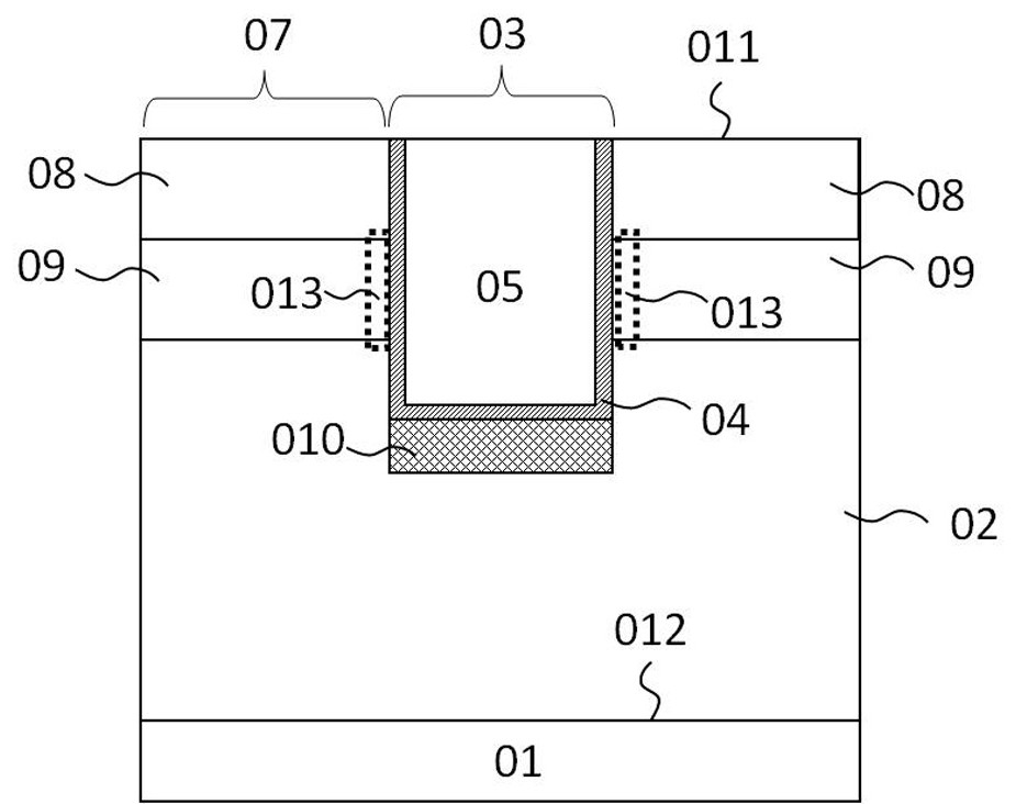
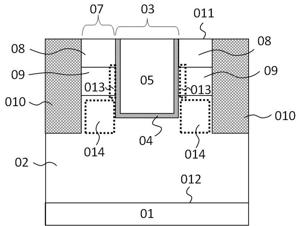
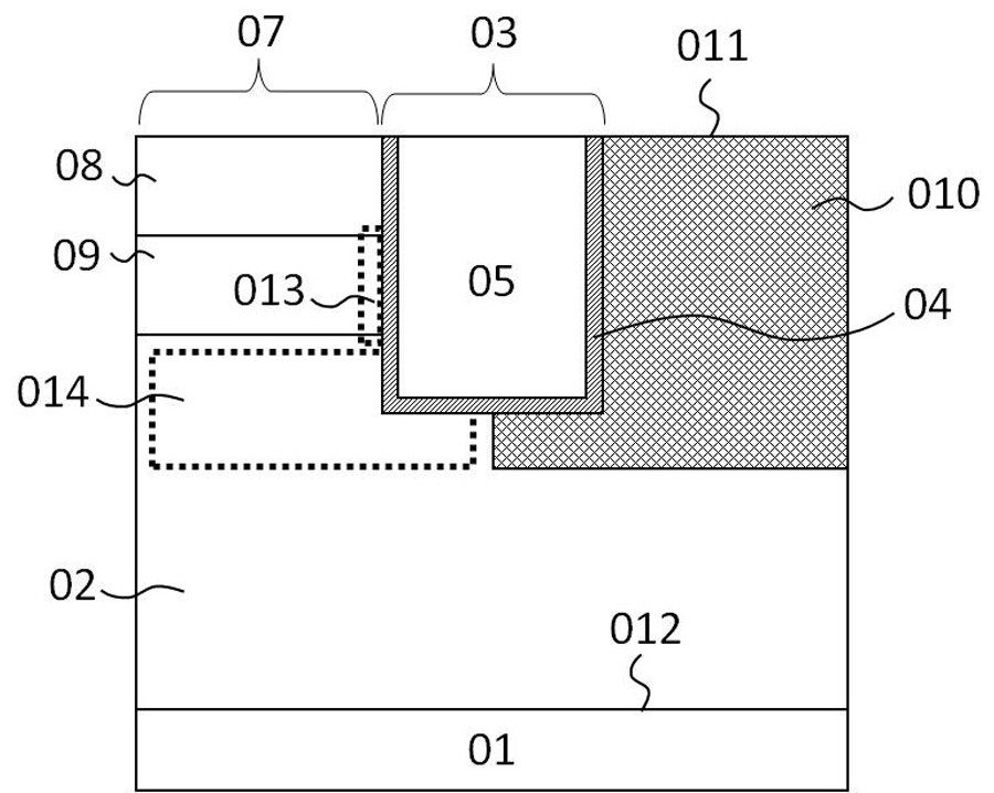
[0038] Specific embodiments of the present invention will be described in detail below in conjunction with the accompanying drawings. It should be noted that the embodiments described here are only for illustration, not for limiting the present invention. In the following description, numerous specific details are set forth in order to provide a thorough understanding of the present invention. However, it will be understood by one of ordinary skill in the art that these specific details are not required to practice the present invention. Additionally, in some embodiments, well-known circuits, materials or methods have not been described in detail in order not to obscure the present invention.

[0039] Throughout this specification, reference to "one embodiment," "an embodiment," "an example," or "example" means that a particular feature, structure, or characteristic described in connection with the embodiment or example is included in the present invention. In at least one em...


PUM


Abstract

The invention provides a trench gate MOSFET device with an electric field shielding structure, which comprises a substrate, a source electrode, a drain electrode, a gate trench, the electric field shielding structure, source electrode regions, a semiconductor region with a first conduction type, and one or more electric field shielding structures with a second conduction type positioned below the surface of the semiconductor region, the electric field shielding structures intersect with the side wall of the gate trench at an angle, and the source electrode regions are positioned on two sides or the periphery of the gate trench, and are divided into a plurality of source sub-regions by an electric field shielding structure. By arranging one or more electric field shielding structures intersecting with the side wall of the gate trench and reasonably arranging the arrangement mode of the electric field shielding structures, the cell size of the device can be effectively reduced, the channel density and the device conduction current density can be improved, the specific on-resistance of the device can be reduced, and the device conduction performance can be improved; meanwhile, the electric field shielding effect is enhanced, the electric field intensity in the gate oxide layer is reduced, and the long-term working stability and reliability of the device are improved.

Description

technical field [0001] The invention relates to a semiconductor device, in particular to a trench gate MOSFET device with an electric field shielding structure. Background technique [0002] The performance of traditional silicon-based semiconductor devices has gradually approached the physical limit of materials, and devices made of third-generation semiconductor materials represented by silicon carbide have excellent working capabilities such as high frequency, high voltage, high temperature resistance, and radiation resistance. Achieve higher power density and higher efficiency. [0003] As a representative of SiC (silicon carbide) switching devices, trench gate MOSFET devices have the advantages of low switching loss, high operating frequency, easy driving, and suitable for parallel use. They have gradually been used in electric vehicles, charging piles, new energy power generation, industrial control , Flexible DC transmission and other application scenarios have been ...

Claims


Application Information

Patent Timeline
Patent Type & Authority Applications(China)
IPC IPC(8): H01L29/78H01L29/06H01L21/04
CPCH01L29/7813H01L29/0696H01L29/0619H01L21/0445H01L29/66068H01L29/1095H01L29/0869H01L29/0623H01L29/4238H01L29/66734H01L29/1608H01L29/0607H01L29/41741H01L29/41775
Inventor 任娜盛况
Owner ZHEJIANG UNIV HANGZHOU GLOBAL SCI & TECH INNOVATION CENT
Why Eureka
Try Eureka