
A process method for improving the performance of trench mos structure schottky diode

A Schottky diode, MOS structure technology, applied in semiconductor devices, electrical components, circuits, etc., can solve the problems of reducing device performance, hidden dangers of use reliability, etc., to reduce charge density, reduce difficulty, and improve resistance to reverse waves. The effect of surge ability

Active Publication Date: 2022-03-11
江苏新顺微电子股份有限公司
View PDF16 Cites 0 Cited by
  • Summary
  • Abstract
  • Description
  • Claims
  • Application Information

AI Technical Summary

Problems solved by technology

This drift voltage brings certain hidden dangers to the reliability of the product. In order to ensure that the minimum breakdown voltage meets the requirements, it is necessary to increase the breakdown value to ensure sufficient redundancy, which also reduces the performance of the device to a certain extent.

Method used


Image

  • A process method for improving the performance of trench mos structure schottky diode
  • A process method for improving the performance of trench mos structure schottky diode
  • A process method for improving the performance of trench mos structure schottky diode

Examples


specific Embodiment 1

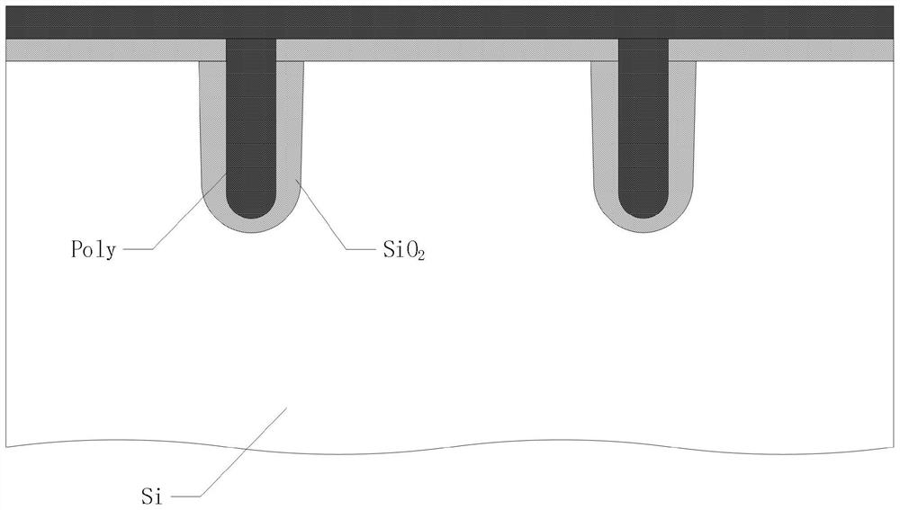
[0046] Specific embodiment 1, see Figure 2 to Figure 7 , a process method for improving the performance of a trench MOS structure Schottky diode. The oxide dielectric layer (oxygen-doped polysilicon layer 2, silicon nitride layer 3 and undoped polysilicon layer) required in the trench MOS structure is thermally oxidized and grown The silicon dioxide layer three) total thickness in Taking the left and right products as an example, the method includes the following steps:

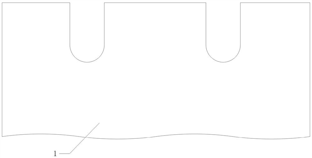
[0047] Step 1: Take the silicon substrate 1 that has undergone groove etching, the depth of the groove is 2.5 μm-4.5 μm, and use hydrofluoric acid etching solution wet process to remove the silicon dioxide on the front side of the silicon substrate as a mask layer for silicon groove etching. silicon. See figure 1 .

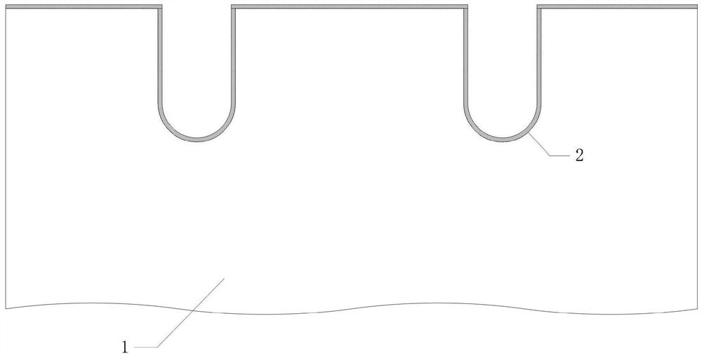
[0048] Step 2: Deposit and grow a thin layer of oxygen-doped polysilicon layer 2 on the aforementioned silicon substrate 1 by LPCVD process; during the process of film deposition, the cavit...


PUM

PropertyMeasurementUnit
electrical resistivityaaaaaaaaaa
thicknessaaaaaaaaaa
electrical resistivityaaaaaaaaaa

Abstract

The present invention relates to the field of semiconductors. A process method for improving the performance of trench MOS structure Schottky diodes, step 1, take the silicon substrate that has completed trench etching, and remove the silicon dioxide layer and other dielectric layers on the silicon surface of the front side of the silicon substrate by wet process; step Two, adopt LPCVD process to deposit and grow a thin layer of oxygen-doped polysilicon layer; Step 3, adopt LPCVD process to deposit a thin layer of silicon nitride layer; Step 4, adopt LPCVD process to deposit a layer of non-doped polysilicon layer; Step 5 , use the furnace tube thermal oxidation process to oxidize the deposited polysilicon layer, and react to form silicon dioxide; step 6, use the CVD process to deposit in-situ doped polysilicon, and finally obtain the silicon trench MOS structure required by the device . The invention improves the thickness uniformity of the dielectric layer, reduces defects generated during the growth process of the dielectric layer, reduces the charge density in the dielectric layer, and improves device performance.

Description

technical field [0001] The invention relates to the mechanical field, in particular to a method for manufacturing a diode device. Background technique [0002] Silicon trench MOS structure Schottky diode is a new type of low power consumption Schottky diode silicon rectifier device. Compared with ordinary planar process Schottky diodes, it adopts silicon trench MOS structure, which reduces the forward voltage. The power consumption of the device can be reduced. The reason why the silicon trench MOS structure Schottky diode can obtain a lower forward voltage drop is that the expansion of the depletion layer on the semiconductor side of the silicon trench MOS structure realizes the electric field shielding of the Schottky junction and improves the The reverse breakdown voltage of the Schottky junction also reduces the reverse leakage of the Schottky junction; at the same time, the oxide dielectric layer in the silicon trench MOS structure has a voltage divider for the reverse...

Claims


Application Information

Patent Timeline
Patent Type & Authority Patents(China)
IPC IPC(8): H01L21/329H01L21/28H01L29/872
CPCH01L29/66143H01L21/28229H01L21/28194H01L29/8725
Inventor 陈晓伦许柏松韩笑孟军朱涛
Owner 江苏新顺微电子股份有限公司
Learn More