Supercharge Your Innovation With Domain-Expert AI Agents!

4H-SiC Schottky diode based on diamond terminal structure and manufacturing method

A Schottky diode and terminal structure technology, which is applied in semiconductor/solid-state device manufacturing, electrical components, circuits, etc., can solve the problems of device leakage current increase, device performance degradation, etc., to reduce electric field concentration and improve reliability , Improve the effect of reverse pressure resistance

Pending Publication Date: 2021-10-26
浙江芯科半导体有限公司
View PDF0 Cites 1 Cited by
  • Summary
  • Abstract
  • Description
  • Claims
  • Application Information

AI Technical Summary

Problems solved by technology

However, due to the actual process error, in reliability tests such as high temperature reverse bias and hot flash reverse bias, the electric field concentration phenomenon in the metal edge region of the SiC Schottky diode using the P-type SiC terminal protection area is still relatively obvious, resulting in device failure. Leakage current increases and device performance degrades

Method used


Image

  • 4H-SiC Schottky diode based on diamond terminal structure and manufacturing method
  • 4H-SiC Schottky diode based on diamond terminal structure and manufacturing method
  • 4H-SiC Schottky diode based on diamond terminal structure and manufacturing method

Examples


Embodiment 1

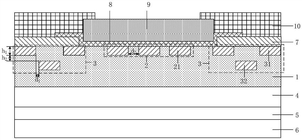
[0045] See figure 1 , figure 1 A schematic structural diagram of a 4H-SiC Schottky diode based on a diamond termination structure provided by an embodiment of the present invention. The 4H-SiC Schottky diode includes: SiC epitaxial layer 1, active region 2, terminal region 3, SiC substrate 4, ohmic contact metal layer 5, first contact layer 6, first passivation layer 7, Schottky base contact metal layer 8 , second contact layer 9 and second passivation layer 10 .

[0046] Specifically, the material of the SiC epitaxial layer 1 includes N-type SiC or P-type SiC.

[0047] The active region 2 is located in the surface layer of the SiC epitaxial layer 1 and exposed from the surface of the SiC epitaxial layer 1 .

[0048]In a specific embodiment, the active region 2 includes several active region diamond structures 21 arranged at intervals, and a pn junction is formed between the active region diamond structures 21 and the SiC epitaxial layer 1 . Specifically, the diamond struc...

Embodiment 2

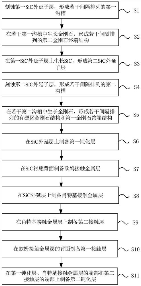
[0065] On the basis of Example 1, please refer to figure 2 and Figure 3a-Figure 3k , figure 2 A schematic flow chart of a method for manufacturing a 4H-SiC Schottky diode based on a diamond termination structure provided by an embodiment of the present invention, Figure 3a-Figure 3k A process schematic diagram of a method for manufacturing a 4H-SiC Schottky diode based on a diamond termination structure provided by an embodiment of the present invention, the method includes steps:

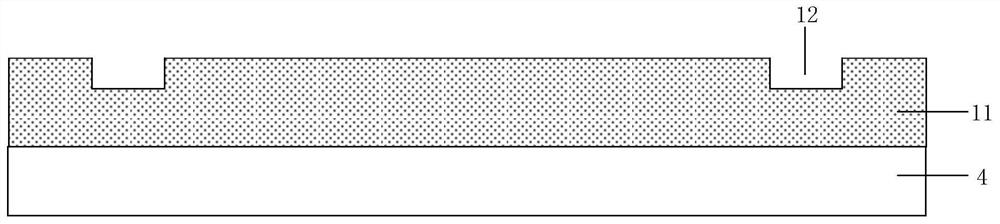
[0066] S1. Etching the first SiC epitaxial sublayer 11 to form a number of first trenches 12 arranged at intervals, please refer to Figure 3a .

[0067] First, a sample is obtained, the sample includes a SiC substrate 4 and a first SiC epitaxial sublayer 11 , and the first SiC epitaxial sublayer 11 is located on the SiC substrate 4 . The material of the first SiC epitaxial sublayer 11 is N-type SiC or P-type SiC, and the SiC in the SiC substrate 4 and the first SiC epitaxial sublayer 11 ar...


PUM

PropertyMeasurementUnit
Thicknessaaaaaaaaaa

Abstract

The invention relates to a 4H-SiC Schottky diode based on a diamond terminal structure and a manufacturing method. The Schottky diode comprises a SiC epitaxial layer; an active region, located in the surface layer of the SiC epitaxial layer; and a terminal area, located in the SiC epitaxial layer and located on the two sides of the active area. The terminal area comprises a plurality of first diamond terminal structures and a plurality of second diamond terminal structures, the first diamond terminal structures are arranged at intervals, and the second diamond terminal structures are arranged at intervals; the plurality of first diamond terminal structures and the plurality of second diamond terminal structures are alternately distributed up and down, and pn junctions are formed between the plurality of first diamond terminal structures and the SiC epitaxial layer and between the plurality of second diamond terminal structures and the SiC epitaxial layer. A surface electric field in the Schottky diode is intensively and gradually introduced into a device body, so that the phenomenon that the device is broken down in advance is avoided, the reliability of the device is improved, and the reverse voltage endurance capability of the device under normal static characteristics is improved.

Description

technical field [0001] The invention belongs to the technical field of semiconductor device structure and manufacture, and in particular relates to a 4H-SiC Schottky diode based on a diamond terminal structure and a manufacturing method. Background technique [0002] The new-generation semiconductor material silicon carbide (SiC) material has many advantages, such as large band gap, high critical breakdown field strength, high thermal conductivity, high saturation electron drift velocity and low dielectric constant. In recent years, the application range of SiC Schottky diodes (SBDs) with higher operating frequency, smaller cell size and lower power consumption has been continuously expanded as the demand has grown. Typical applications of SiC Schottky diodes include rectification circuits, power protection circuits, voltage clamping circuits, etc. In addition, the reverse recovery time of SiC Schottky diodes is smaller than that of fast recovery diodes or ultra-fast recove...

Claims


Application Information

Patent Timeline
IPC IPC(8): H01L29/872H01L29/06H01L21/329
CPCH01L29/872H01L29/0607H01L29/0615H01L29/6606
Inventor 李京波王小周赵艳
Owner 浙江芯科半导体有限公司
Features
  • R&D
  • Intellectual Property
  • Life Sciences
  • Materials
  • Tech Scout
  • Unparalleled Data Quality
  • Higher Quality Content
  • 60% Fewer Hallucinations
Learn More