Surface treatment process of integrated circuit lead frame
A lead frame, integrated circuit technology, applied in the electrolysis process, electrolysis components, cells, etc., can solve the problems of incurability, threat to workers' health, environmental pollution, etc., and achieve strong solderability, high electroplating efficiency, and good solution stability. Effect
- Summary
- Abstract
- Description
- Claims
- Application Information
AI Technical Summary
Problems solved by technology
Method used
Image
Examples
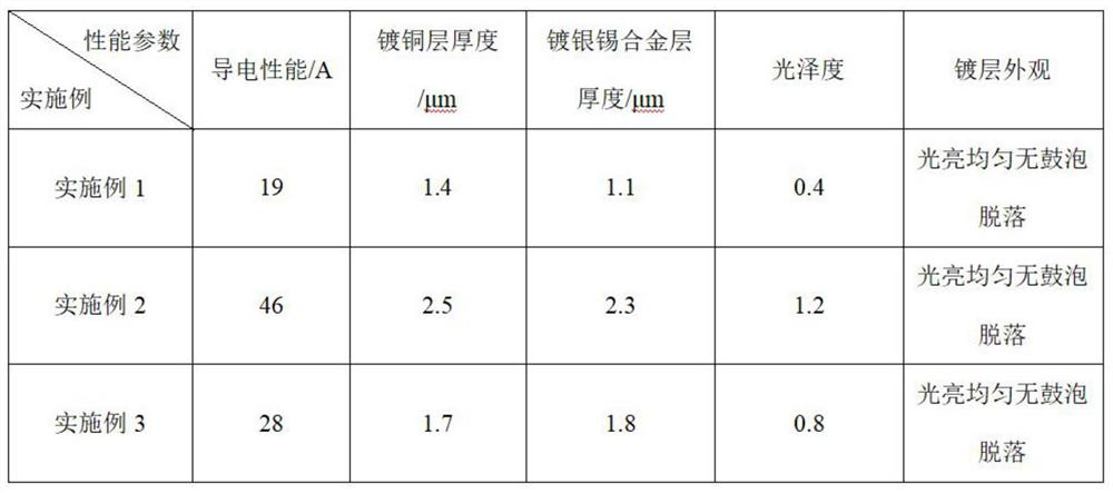
Embodiment 1
[0022] This embodiment provides a surface treatment process for an integrated circuit lead frame, which mainly includes the following steps:
[0023] (1) Degreasing: Ultrasonic degreasing and bipolar degreasing are performed on the IC lead frame first, and CY-01 degreasing powder with a concentration of 85g / L is used for both, the temperature is 50°C, and the time is 6-10min / m;
[0024] (2) Acid activation: acid-activate the degreased integrated circuit lead frame with 65ml / L of sulfuric acid at room temperature, the acid activation time is 6-10min / m, then rinse with pure water and dry;
[0025] (3) Copper plating: put the integrated circuit lead frame after acid activation into a Hall tank equipped with copper plating solution for electrodeposition, the time is 6-10min / m, and the copper plating solution mainly includes the following components : Copper Tetrafluoroborate 50g / L, Disodium EDTA 5g / L, Potassium Sulfate 15g / L, Sodium Thiosulfate 20mg / L, then wash with pure water an...
Embodiment 2
[0032] This embodiment provides a surface treatment process for an integrated circuit lead frame, which mainly includes the following steps:
[0033] (1) Degreasing: Ultrasonic degreasing and bipolar degreasing are carried out on the lead frame of the integrated circuit first, and CY-01 degreasing powder with a concentration of 95g / L is selected, the temperature is 60°C, and the time is 10min / m;
[0034] (2) Acid activation: carry out acid activation at room temperature with 75ml / L sulfuric acid on the degreased integrated circuit lead frame, the acid activation time is 6-10min / m, then rinse with pure water and dry;
[0035] (3) Copper plating: put the integrated circuit lead frame after acid activation into a Hall tank equipped with copper plating solution for electrodeposition, the time is 6-10min / m, and the copper plating solution mainly includes the following components : Copper tetrafluoroborate 100g / L, disodium edetate 7.5g / L, sodium citrate 7.5g / L, conductive salt potas...
Embodiment 3
[0042] This embodiment provides a surface treatment process for an integrated circuit lead frame, which mainly includes the following steps:
[0043] (1) Degreasing: Ultrasonic degreasing and bipolar degreasing are carried out on the lead frame of the integrated circuit first, and CY-01 degreasing powder with a concentration of 90g / L is selected, the temperature is 55°C, and the time is 6-10min / m;
[0044] (2) Acid activation: carry out acid activation at room temperature with 70ml / L sulfuric acid on the degreased integrated circuit lead frame, the acid activation time is 6-10min / m, then rinse with pure water and dry;
[0045] (3) Copper plating: put the integrated circuit lead frame after acid activation into a Hall tank equipped with copper plating solution for electrodeposition, the time is 6-10min / m, and the copper plating solution mainly includes the following components : Copper tetrafluoroborate 75g / L, sodium citrate 10g / L, potassium nitrate 22.5g / L, sodium benzoate 35m...
PUM
| Property | Measurement | Unit |
|---|---|---|
| Current density | aaaaa | aaaaa |
Abstract
Description
Claims
Application Information
 - R&D
- Intellectual Property
- Life Sciences
- Materials
- Tech Scout
- Unparalleled Data Quality
- Higher Quality Content
- 60% Fewer Hallucinations
Browse by: Latest US Patents, China's latest patents, Technical Efficacy Thesaurus, Application Domain, Technology Topic, Popular Technical Reports.
© 2025 PatSnap. All rights reserved.Legal|Privacy policy|Modern Slavery Act Transparency Statement|Sitemap|About US| Contact US: help@patsnap.com

