Ferromagnetic silicon carbide crystal and preparation method thereof

A silicon carbide and ferromagnetic technology, applied in the field of ferromagnetic silicon carbide crystals and its preparation, to achieve high magnetoelectric conversion efficiency, uniform P-type elements, and uniform stress

Active Publication Date: 2021-11-30
SICC CO LTD
View PDF8 Cites 0 Cited by
  • Summary
  • Abstract
  • Description
  • Claims
  • Application Information

AI Technical Summary

Problems solved by technology

With the continuous development of information technology and the rapid improvement of processing and transmission speeds, the existing semiconductor integrated circuits are difficult to meet people's needs

Method used


Image

  • Ferromagnetic silicon carbide crystal and preparation method thereof
  • Ferromagnetic silicon carbide crystal and preparation method thereof
  • Ferromagnetic silicon carbide crystal and preparation method thereof

Examples


Embodiment 1

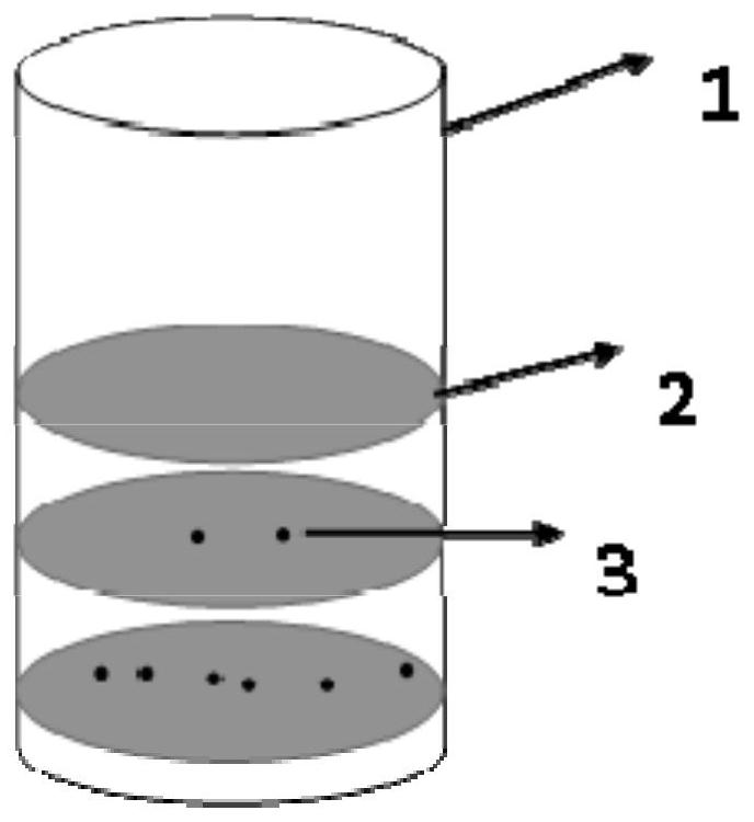
[0077] by figure 1 The illustrated embodiment of three silicon carbide wafers is to illustrate the method for preparing ferromagnetic silicon carbide crystals of the present application, but is not limited to three silicon carbide wafers.

[0078]As an embodiment, the preparation method of ferromagnetic silicon carbide crystal comprises the following steps:

[0079] 1) Assembly steps: medium frequency induction heating is used for crystal growth, and the crucible is assembled before heating. The specific assembly is to adopt a layered charging method, and Al with a boiling point (decomposition point) of 2200 ° C 4 C 3 Place 0.3g between the upper and middle silicon carbide wafers, and 0.6g between the middle and lower layers; the thicknesses of the upper silicon carbide wafer, middle silicon carbide wafer, and lower silicon carbide wafer are 500μm, 450μm, and 400μm in sequence;

[0080] 2) Crystal growth:

[0081] a. Vacuum removal: vacuum the furnace to 10 -6 Below mbar, ...

Embodiment 2

[0089] The difference between this embodiment and embodiment 1 is that the Al in the raw material is adjusted 4 C 3 The concentrations of the doped aluminum ions and the generated holes in the prepared silicon carbide crystals were tested respectively, and the ferromagnetic silicon carbide crystals 2#-5# were respectively prepared, compared with the ferromagnetic silicon carbide crystals D1#-D2# , see Table 1 for details.

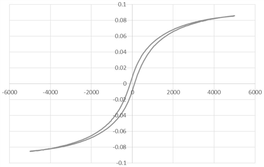
[0090] Test the obtained ferromagnetic silicon carbide crystals 1#-5# and comparative ferromagnetic silicon carbide crystals D1#-D2# respectively: magnetization curve (can judge whether it is ferromagnetic, saturation magnetization value), SIMS test aluminum ion concentration, Hall test carrier concentration, resistivity and its distribution, and XRD.

[0091] Take the test result of ferromagnetic silicon carbide crystal 1# as an example to illustrate the performance of the ferromagnetic silicon carbide crystal of the present application:

[0092] figu...

Embodiment 3

[0101] The method for preparing ferromagnetic silicon carbide crystals in this embodiment differs from that in Example 1 in that:

[0102] 3) Cavitation control: After growing for 20 hours in step c2, open the nitrogen valve to control the flow rate to 4 sccm / min, and evenly pass it into the growth chamber for 30 hours until the crystal growth process is completed, that is, the ferromagnetic silicon carbide crystal 6# is obtained.

[0103] Since nitrogen doping introduces a gap with the atomic diameter of silicon carbide to enter holes, the introduction of holes and the dopant atoms work together to contribute to the ferromagnetism of silicon carbide crystals.


PUM

PropertyMeasurementUnit
electrical resistivityaaaaaaaaaa

Abstract

The invention discloses a ferromagnetic silicon carbide crystal and a preparation method thereof, and belongs to the field of semiconductor materials. The ferromagnetic silicon carbide crystal has P-type doped ions and holes, and the concentration ratio of the P-type doped ions to the holes is 1: (3-10), so that the silicon carbide crystal is the ferromagnetic P-type silicon carbide crystal. The silicon carbide crystal can reach relatively high saturation magnetization intensity at room temperature after passing through a magnetic field so as to meet the requirement of room temperature on ferromagnetic intensity in the semiconductor silicon carbide crystal.

Description

technical field [0001] The application relates to a ferromagnetic silicon carbide crystal and a preparation method thereof, belonging to the field of semiconductor materials. Background technique [0002] Semiconductor devices mainly use the charge properties of electrons to process and transmit information, while the information storage function is realized by using ferromagnetism, that is, the spin properties of electrons. With the continuous development of information technology and the rapid improvement of processing and transmission speeds, existing semiconductor integrated circuits are difficult to meet people's needs. If the charge and spin properties of electrons can be combined, there will undoubtedly be a huge technological breakthrough. Based on turning this ideal into reality, spintronics came into being. [0003] As a third-generation semiconductor with excellent performance, SiC has good application prospects in the fields of high-frequency and high-power dev...

Claims


Application Information

Patent Timeline
Patent Type & Authority Applications(China)
IPC IPC(8): C30B29/36C30B28/12C30B23/00
CPCC30B29/36C30B28/12C30B23/00
Inventor 张宁石志强姜彦鹏高超杨晓俐李博刘鹏飞
Owner SICC CO LTD
Why Eureka
Try Eureka