Check patentability & draft patents in minutes with Patsnap Eureka AI!

Externally modulated laser array monolithic photonic integrated chip

A laser array and photonic integration technology, applied in the semiconductor field, can solve the problems of high cost, high power consumption of EML, and the inability of discrete TOSA components to meet the demand, and achieve the effect of low cost and small size

Pending Publication Date: 2021-12-03
ZHEJIANG UNIV
View PDF3 Cites 0 Cited by
  • Summary
  • Abstract
  • Description
  • Claims
  • Application Information

AI Technical Summary

Problems solved by technology

Because EML adopts DC modulation, there is no chirp effect caused by carrier fluctuations, so the dispersion will be relatively low, which is more conducive to long-distance and high-speed transmission, but EML consumes more power and costs more.
[0005] To sum up, the discrete TOSA components based on DML and EML in related technologies cannot meet the requirements of next-generation 800G optical communications. Therefore, how to provide a TOSA component with low power consumption, low cost and high transmission rate has become an urgent problem to be solved. one of the technical problems

Method used


Image

  • Externally modulated laser array monolithic photonic integrated chip

Examples


Embodiment Construction

[0028] Embodiments of the present invention are described in detail below, examples of which are shown in the drawings, wherein the same or similar reference numerals designate the same or similar elements or elements having the same or similar functions throughout. The embodiments described below by referring to the figures are exemplary and are intended to explain the present invention and should not be construed as limiting the present invention.

[0029] The following describes an externally adjusted laser array monolithic photonic integrated chip proposed according to an embodiment of the present invention with reference to the accompanying drawings.

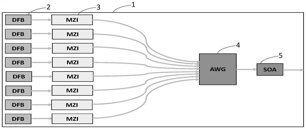
[0030] figure 1 It is a schematic diagram of an externally adjusted laser array monolithic photonic integrated chip according to an embodiment of the present invention.

[0031] Such as figure 1 As shown, the externally adjusted laser array monolithic photonic integrated chip includes a semiconductor material substrate 1,...


PUM

PropertyMeasurementUnit
wavelengthaaaaaaaaaa

Abstract

The invention discloses an externally modulated laser array monolithic photonic integrated chip. The chip comprises a semiconductor material substrate, eight distributed feedback lasers (DFB), eight Mach-Zehnder electro-optical modulators (MZI), an array waveguide grating (AWG) and a semiconductor optical amplifier (SOA). The distributed feedback lasers, the Mach-Zehnder electro-optical modulators, the array waveguide grating and the semiconductor optical amplifier are integrated on the same semiconductor material substrate, and any two adjacent components are connected through a passive waveguide structure. The first end of each Mach-Zehnder electro-optical modulator (MZI) is connected with the corresponding distributed feedback laser (DFB), the second end of each Mach-Zehnder electro-optical modulator (MZI) is connected with the first end of the array waveguide grating (AWG), and the second end of the array waveguide grating (AWG) is connected with the semiconductor optical amplifier (SOA). The chip is compact in size, low in packaging cost and low in power consumption, and can realize 800 Gbps high-speed data transmission.

Description

technical field [0001] The invention relates to the technical field of semiconductors, in particular to an externally adjusted laser array monolithic photonic integrated chip. Background technique [0002] At present, the rapid development of emerging Internet applications such as big data, cloud computing, cloud storage, and the Internet of Things has an increasing demand for data broadband transmission, resulting in an exponential increase in data center traffic, which greatly increases the demand for high-speed optical modules. Promote the development of high-speed optoelectronic devices and chips. The core optoelectronic devices of the optical module are the optical transmitting assembly (TOSA) and the optical receiving assembly (ROSA). The working principle of the Optical Transmitting Assembly (TOSA) is: the laser signal emitted by multiple semiconductor lasers is coupled to a single fiber output port through a wavelength division multiplexing chip (MUX), such as an ar...

Claims


Application Information

Patent Timeline
Patent Type & Authority Applications(China)
IPC IPC(8): H01S5/026H01S5/06H01S5/12H01S5/40H04B10/50
CPCH01S5/4025H01S5/0265H01S5/12H01S5/06H04B10/503
Inventor 熊婉姝姚偌云李玉苗吉晨
Owner ZHEJIANG UNIV
Features
  • R&D
  • Intellectual Property
  • Life Sciences
  • Materials
  • Tech Scout
  • Unparalleled Data Quality
  • Higher Quality Content
  • 60% Fewer Hallucinations
Learn More