Layered micro-nano composite structure for enhancing boiling heat transfer, and processing method thereof
A composite structure and enhanced boiling technology, which is applied in indirect heat exchangers, lighting and heating equipment, cooling/ventilation/heating transformation, etc., can solve the complexity of the micro-nano composite structure process, the blockage of liquid supply channels and heat transfer, and the Difficult heat transfer enhancement effects and other issues, to achieve the effect of delaying heat transfer deterioration, increasing critical heat flux density, and increasing actual heat transfer area
- Summary
- Abstract
- Description
- Claims
- Application Information
AI Technical Summary
Problems solved by technology
Method used
Image
Examples
Embodiment 1
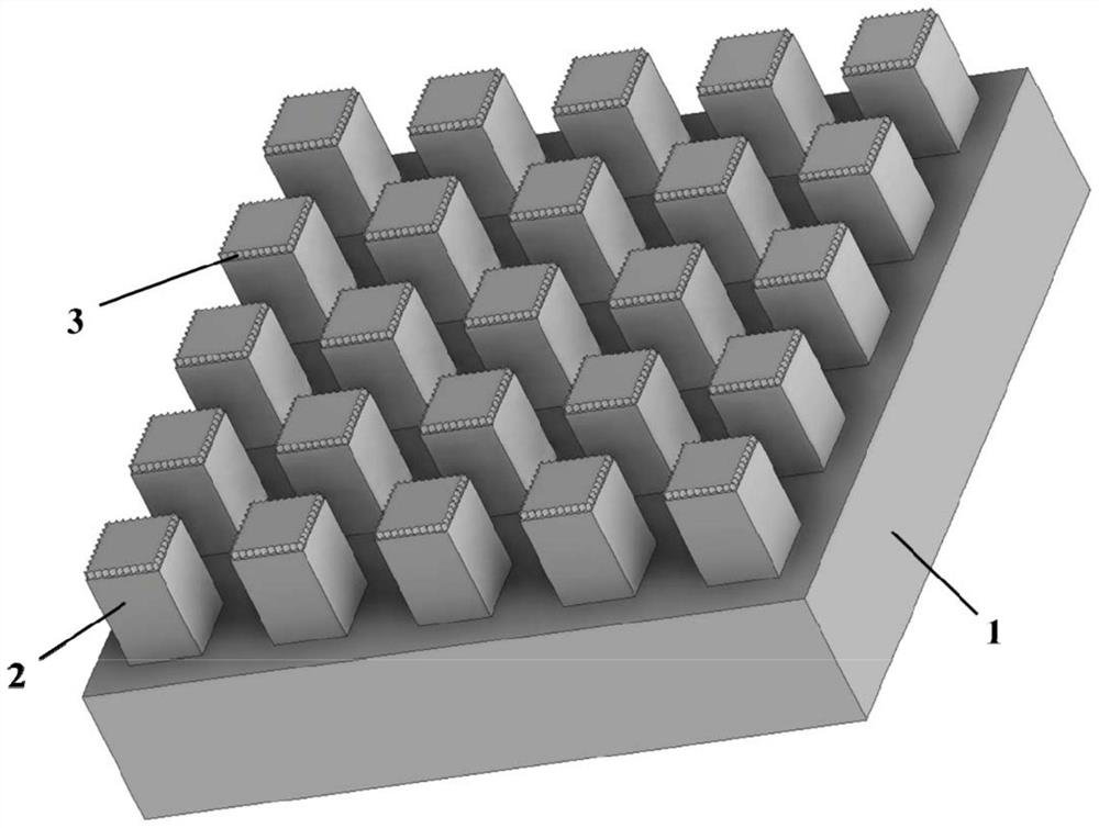
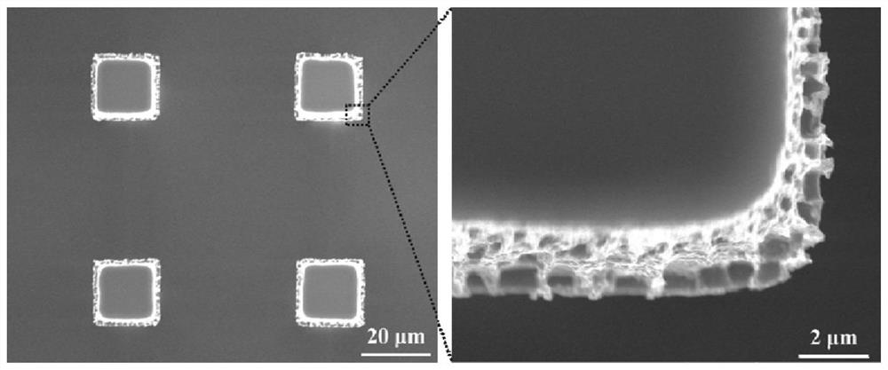
[0035] Goal: To etch a regular array of square column microstructures with a column width of 20 μm, a column height of 120 μm, and a center-to-center distance of 60 μm, and to etch nanoscale holes on the four edges of the top surface of the square columns.
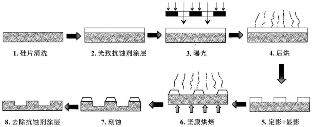
[0036] Step 1: Design a corresponding mask pattern according to the etching target, and process the mask.
[0037] Step 2: Pretreat the silicon wafer with HMDS for 10 minutes; then stick it on the glue homogenizer, rotate it forward at a speed of 600r / min for 6s, and reverse it at a speed of 4000r / min for 30s, so that the photoresist AZ6130 Evenly coat the front side of the silicon wafer with a coating thickness of 7.5 μm; then place the silicon wafer on a contact hot plate at 100°C and dry for 5 minutes to obtain a relatively strong photoresist layer. Then place the silicon wafer on the MA6 photolithography machine for exposure for 23s, and place it in 2.38% TMAH developer for 150s to complete the developing process. Aft...
Embodiment 2
[0039] Objective: To etch a regular array of square column microstructures with a column width of 50 μm, a column height of 60 μm, and a center-to-center distance of 100 μm, and to etch nanoscale holes on the four edges of the top surface of the square columns.
[0040] Step 1: Design a corresponding mask pattern according to the etching target, and process the mask.
[0041]Step 2: pretreat the silicon wafer with HMDS for 10 minutes; then stick it on the glue homogenizer, rotate it forward at a speed of 600r / min for 6s, and reverse it at a speed of 1000r / min for 30s, so that the photoresist AZ6130 Evenly coat the front side of the silicon wafer with a coating thickness of 5.2 μm; then place the silicon wafer on a contact hot plate at 100°C and dry for 5 minutes to obtain a relatively strong photoresist layer. Then put the silicon wafer on the MA6 photolithography machine for 4.2s exposure, and put it in the 3038 developer solution for 70s to complete the development process. ...
Embodiment 3
[0044] Goal: To etch a regular array of square column microstructures with a column width of 100 μm, a column height of 60 μm, and a center-to-center distance of 200 μm, and to etch nanoscale holes on the four edges of the top surface of the square columns.
[0045] Step 1: Design a corresponding mask pattern according to the etching target, and process the mask.
[0046] Step 2: pretreat the silicon wafer with HMDS for 10 minutes; then stick it on the glue homogenizer, rotate it forward at a speed of 600r / min for 6s, and reverse it at a speed of 1000r / min for 30s, so that the photoresist AZ6130 Evenly coat the front side of the silicon wafer with a coating thickness of 5.2 μm; then place the silicon wafer on a contact hot plate at 100°C and dry for 5 minutes to obtain a relatively strong photoresist layer. Then put the silicon wafer on the MA6 photolithography machine for 4.2s exposure, and put it in the 3038 developer solution for 70s to complete the development process. Af...
PUM
| Property | Measurement | Unit |
|---|---|---|
| Thickness | aaaaa | aaaaa |
| Diameter | aaaaa | aaaaa |
| Column height | aaaaa | aaaaa |
Abstract
Description
Claims
Application Information


