Manufacturing method of super junction device

A manufacturing method and super junction technology, applied in semiconductor/solid-state device manufacturing, semiconductor devices, electrical components, etc., can solve the problems of gate dielectric layer damage, inability to form a protective effect, and inability to prevent polysilicon gate impurities from accumulating on the silicon surface, etc. To achieve the effect of preventing the external expansion of doping impurities and preventing damage

Pending Publication Date: 2022-02-08
SHANGHAI HUAHONG GRACE SEMICON MFG CORP
View PDF6 Cites 2 Cited by
  • Summary
  • Abstract
  • Description
  • Claims
  • Application Information

AI Technical Summary

Problems solved by technology

In this method, the polysilicon gate is formed before the super junction structure, which will directly expose the surface of the polysilicon gate after the first planarization, and the polysilicon gate is usually a heavily doped structure such as N-type heavily doped structure, at this time, the doping impurities of the polysilicon gate, such as phosphorus or arsenic, are prone to outspread (Out Doping) at high temperatures, especially in the process of silicon oxide film formation, because the solid solubility of P and As in the oxide layer is far away. Smaller than silicon, the thermal oxidation process has a repelling effect on P and As, resulting in the accumulation of N-type doping elements out of Out Doping in the polysilicon gate during the thermal oxidation process and diffusion on the Si surface; in addition, the gate dielectric on both sides of the polysilicon gate The top surface of the layer is also exposed, making the gate dielectric layer vulnerable to damage
[0022] An improved method is to etch the polysilicon gate in advance to form a groove after the formation of the polysilicon gate, and then use the ONO of the second hard mask layer to form the second hard mask layer defining the super junction trench. The bottom oxide layer in the structure is used to fill the groove and act as a cap layer on the top of the polysilicon gate. In this method, the bottom oxide layer is usually formed by a thermal oxidation process. The thermal process in the formation process of the bottom oxide layer itself will make the impurities of the polysilicon gate Outward expansion occurs. At this time, it cannot prevent the accumulation of impurities in the outer expansion of the polysilicon gate on the silicon surface, so it cannot form a good protective effect.

Method used


Image

  • Manufacturing method of super junction device
  • Manufacturing method of super junction device
  • Manufacturing method of super junction device

Examples


Embodiment Construction

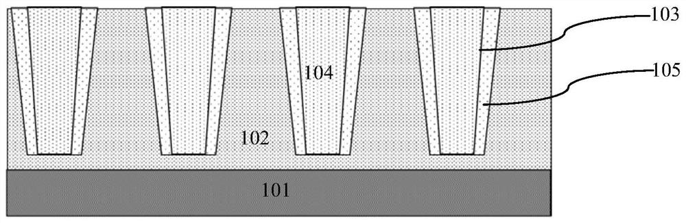
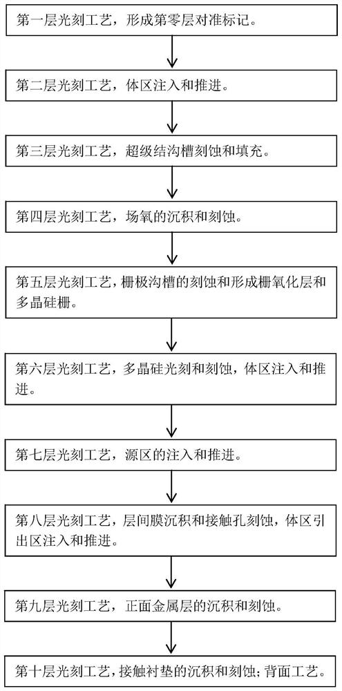
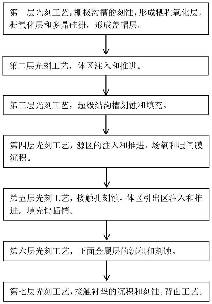
[0089] Such as image 3 Shown is a flowchart of a method for manufacturing a super junction device according to an embodiment of the present invention; image 3 It is described according to the lithography process level. A lithography process level includes multiple specific process steps. In a lithography process level, only the lithography process corresponding to one mask is performed; for example Figure 4A to Figure 4N As shown, it is a schematic diagram of the device structure in each step of the manufacturing method of the super junction device according to the embodiment of the present invention. Before forming the process, the following steps are included:

[0090] Step 1, such as Figure 4A As shown, the gate structure is formed, the gate structure is a trench gate, and the formation process of the trench gate includes:

[0091] A first epitaxial layer 2 with a first conductivity type is provided, and a photolithography process is performed to define a formation r...


PUM


Abstract

The invention discloses a manufacturing method of a super junction device. The method comprises the following steps: step 1, forming a gate structure which is a trench gate, filling a gate trench with a polysilicon gate in the formation process of the trench gate, and performing first flattening to enable the surface of a first epitaxial layer with the trench gate to be a flat surface, wherein the width of the gate trench at the leading-out position of the gate structure meets the requirement of forming a contact hole; step 2, forming a cap layer at the top of the trench gate under the condition that the gate oxide layer outside the gate trench is reserved; and step 3, forming a super junction in the first epitaxial layer which is provided with the cap gate and has the flat surface, and carrying out second flattening. According to the method, on the basis of realizing the full-flat process, the external expansion of doped impurities of the polysilicon gate and the damage to the gate oxide layer can be prevented at the same time.

Description

technical field [0001] The invention relates to a method for manufacturing a semiconductor integrated circuit, in particular to a method for manufacturing a super junction device. Background technique [0002] The super junction is composed of alternately arranged P-type thin layers also called P-type pillars (Pillar) and N-type thin layers also called N-type pillars formed in the semiconductor substrate. Devices using super junctions are super junction devices such as super junction devices. junction MOSFET. The internal reduced surface electric field (Resurf) technology using P-type thin layer and N-type thin layer charge balance can increase the reverse breakdown voltage of the device while maintaining a small on-resistance. [0003] The pillar structure of the PN interval of the super junction is the biggest feature of the super junction. Currently, there are mainly two methods for manufacturing the pillar structure of the PN spacer, one is obtained by multiple epitaxy...

Claims


Application Information

Patent Timeline
Patent Type & Authority Applications(China)
IPC IPC(8): H01L21/336H01L21/28
CPCH01L29/66484H01L29/66734H01L21/28035H01L21/28123
Inventor 李昊
Owner SHANGHAI HUAHONG GRACE SEMICON MFG CORP
Why Eureka
Try Eureka