Preparation method of CZTS thin-film solar cell back electrode with modification layer

A technology for solar cells and modified layers, applied in the field of solar cells, can solve the problems of destroying the stability of Mo electrodes, affecting carrier collection, and falling off of Mo electrodes, so as to improve carrier transport performance, increase photoelectric conversion efficiency, reduce The effect of grain boundary defects

Pending Publication Date: 2022-03-11
HUBEI UNIV OF TECH
View PDF0 Cites 0 Cited by
  • Summary
  • Abstract
  • Description
  • Claims
  • Application Information

AI Technical Summary

Problems solved by technology

In the device structure of CZTS thin film solar cells, the molybdenum substrate back electrode (Mo electrode) will react with the CZTS thin film during the device preparation process to form thicker MoS 2 layer, over thick MoS 2 The layer will not only hinder the transmission of electrons to the Mo electrode, but also destroy the stability of the Mo electrode, and there is a risk that the Mo electrode will fall off after long-term use of the device, resulting in damage or failure of the device.
In addition, due to the large number of grain boundaries in the polycrystalline CZTS film, the carrier scattering is strong, which also affects the collection of carriers in the CZTS film by the back electrode.

Method used


Image

  • Preparation method of CZTS thin-film solar cell back electrode with modification layer
  • Preparation method of CZTS thin-film solar cell back electrode with modification layer
  • Preparation method of CZTS thin-film solar cell back electrode with modification layer

Examples


Embodiment 1

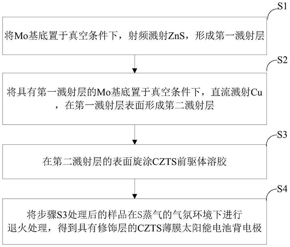
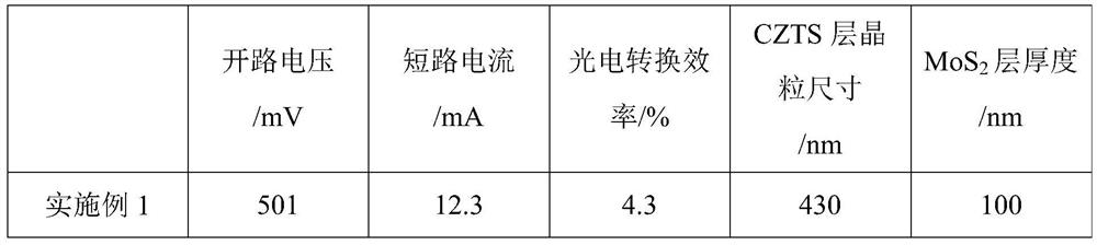
[0030] (1) Place the Mo substrate in a vacuum chamber, use ZnS target radio frequency sputtering to sputter the first sputtering layer, the sputtering power is 80W, the sputtering pressure is 1Pa, and the sputtering time is 2s;

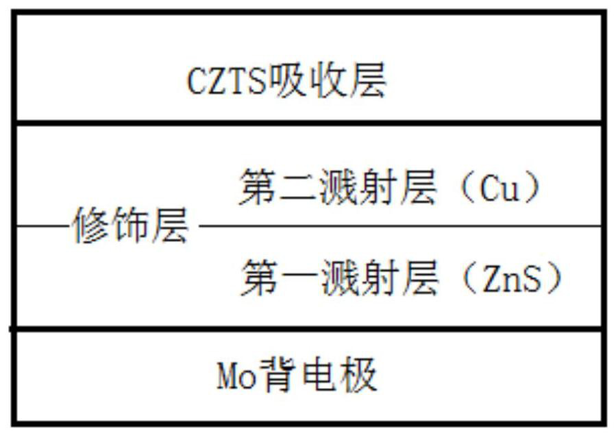
[0031] (2) Place the Mo substrate with the first sputtering layer in a vacuum chamber, and use a Cu target to direct-current sputter the second sputtering layer, the sputtering power is 40W, the sputtering pressure is 1Pa, and the sputtering time is 1s. Mo back electrode with modification layer;

[0032] (3) Prepare CZTS precursor sol at a temperature of 50°C, the solvent is ethylene glycol methyl ether, the additive is triethanolamine (the volume ratio of additive to solvent is 1:50), and the metal salt is Cu, Zn, Sn chloride Compounds, the molar concentrations of metal atoms are: 0.05M, 0.03M and 0.025M. The CZTS precursor sol is spin-coated on the Mo back electrode with the modified layer treated in step (2) to form a CZTS film.

[0033] (4) Plac...

Embodiment 2

[0035] (1) Place the Mo substrate in a vacuum chamber, use ZnS target radio frequency sputtering to sputter the first sputtering layer, the sputtering power is 60W, the sputtering pressure is 0.5Pa, and the sputtering time is 3s;

[0036] (2) Place the Mo substrate with the first sputtering layer in a vacuum chamber, and use a Cu target to direct-current sputter the second sputtering layer, the sputtering power is 30W, the sputtering pressure is 1Pa, and the sputtering time is 1s. Mo back electrode with modification layer;

[0037] (3) Prepare CZTS precursor sol at a temperature of 40°C, the solvent is ethylene glycol methyl ether, the additive is monoethanolamine (the volume ratio of additive to solvent is 1:25), and the metal salt is nitric acid of Cu, Zn, and Sn Compounds, the molar concentrations of metal atoms are: 0.03M, 0.02M and 0.015M. The CZTS precursor sol is spin-coated on the Mo back electrode with the modified layer treated in step (2) to form a CZTS film.

[0...

Embodiment 3

[0040] (1) Place the Mo substrate in a vacuum chamber, use ZnS target radio frequency sputtering for the first sputtering layer, the sputtering power is 40W, the sputtering pressure is 3Pa, and the sputtering time is 5s;

[0041](2) Place the Mo substrate with the first sputtering layer in the vacuum chamber, use the Cu target to sputter the second sputtering layer with direct current, the sputtering power is 20W, the sputtering pressure is 1Pa, and the sputtering time is 2s, the obtained Mo back electrode with modification layer;

[0042] (3) Prepare CZTS precursor sol at a temperature of 60°C, the solvent is N,N-dimethylformamide, the additive is diethanolamine (the volume ratio of additive to solvent is 1:40), and the metal salt is Cu, Zn , Sn sulfate, the molar concentration of metal atoms are: 0.14M, 0.11M and 0.07M. The CZTS precursor sol is spin-coated on the Mo back electrode with the modified layer treated in step (2) to form a CZTS film.

[0043] (4) Place the samp...


PUM

PropertyMeasurementUnit
thicknessaaaaaaaaaa
particle sizeaaaaaaaaaa

Abstract

The invention provides a preparation method of a CZTS thin-film solar cell back electrode with a modification layer, and the method comprises the following steps: firstly, placing a Mo substrate under a vacuum condition, and carrying out the radio-frequency sputtering of ZnS, so as to form a first sputtering layer; secondly, under the vacuum condition, Cu is subjected to direct current sputtering, and a second sputtering layer is formed on the surface of the first sputtering layer; thirdly, spin-coating CZTS precursor sol on the surface of the second sputtering layer; and finally, carrying out annealing treatment under S steam. Wherein the first sputtering layer of the modification layer can be used as an S vapor barrier layer to inhibit vulcanization of the Mo layer and reduce the thickness of MoS2; and the second sputtering layer of the modification layer takes Cu as a raw material for direct current sputtering, so that the crystallization of an upper-layer CZTS precursor is facilitated, and the grain boundary defect of the CZTS is reduced. Besides, the modification layer can form a heavy p + type layer between the CZTS thin film on the upper layer and the Mo electrode on the lower layer, the carrier transmission performance of the contact side of the CZTS layer and the Mo back electrode is improved, and the photoelectric conversion efficiency of the solar cell device is further improved.

Description

technical field [0001] The invention belongs to the technical field of solar cells, and in particular relates to a method for preparing a back electrode of a CZTS thin-film solar cell with a modification layer. Background technique [0002] Copper zinc tin sulfur (Cu 2 ZnSnS 4 , CZTS) are used in solar cell devices because of their cheapness, non-toxicity and suitable energy band structure. At present, the photoelectric conversion efficiency of CZTS thin-film solar cell devices has reached more than 10%, showing a good application prospect. In the device structure of CZTS thin film solar cells, the molybdenum substrate back electrode (Mo electrode) will react with the CZTS thin film during the device preparation process to form thicker MoS 2 layer, over thick MoS 2 The layer will not only hinder the transmission of electrons to the Mo electrode, but also destroy the stability of the Mo electrode. After long-term use of the device, the Mo electrode may fall off, resulting...

Claims


Application Information

Patent Timeline
Patent Type & Authority Applications(China)
IPC IPC(8): H01L31/18H01L31/0224H01L31/0352C23C14/06C23C14/18
CPCH01L31/18H01L31/022441H01L31/03529C23C14/18C23C14/0629Y02P70/50
Inventor 童正夫韩长存刘志锋方黎柳阳王文君谭保华
Owner HUBEI UNIV OF TECH
Why Eureka
Try Eureka