Process method for processing ZrAlO film system on cavity surface of semiconductor chip

A process method and semiconductor technology, applied in semiconductor lasers, metal material coating process, ion implantation plating, etc., can solve the problem of affecting the mechanical properties and adhesion of the film layer, affecting the service life and reliability, affecting the reliability of the laser, etc. problems, to achieve the effect of improving long-term aging ability and antistatic properties, improving product competitiveness and service life, good mechanical properties and adhesion

Pending Publication Date: 2022-03-25
WUHAN GUANGANLUN OPTOELECTRONICS TECH CO LTD
View PDF0 Cites 0 Cited by
  • Summary
  • Abstract
  • Description
  • Claims
  • Application Information

AI Technical Summary

Problems solved by technology

[0002] In the manufacturing process of semiconductor lasers, especially for DFB (Distributed Feedback Laser) lasers, the last step of the process needs to coat the cavity surface of the laser to realize the protection of the cavity surface, and by changing the emissivity of the cavity surface, it is realized for The gain effect of the laser output and the monitoring of the backlight; in addition, the quality of the cavity film layer also directly affects the service life and reliability of the laser. How to design a more reasonable film system and achieve excellent film quality has always been an industry practitioner At the same time, because the current high-speed chip solutions are generally made of Al-containing substrates (ie InGaAlAs) to improve the high-temperature characteristics of the laser, but because Al is easily oxidized, the laser cavity surface will be damaged after cleavage. There will be a risk of being oxidized when exposed to air, and then the cavity surface will be oxidized to form defect accumulation, which will easily form thermal energy accumulation during use, directly affect the mechanical properties and adhesion of the film layer, and then affect the reliability of the laser, leading to its failure

Method used


Image

  • Process method for processing ZrAlO film system on cavity surface of semiconductor chip
  • Process method for processing ZrAlO film system on cavity surface of semiconductor chip
  • Process method for processing ZrAlO film system on cavity surface of semiconductor chip

Examples


Embodiment 1

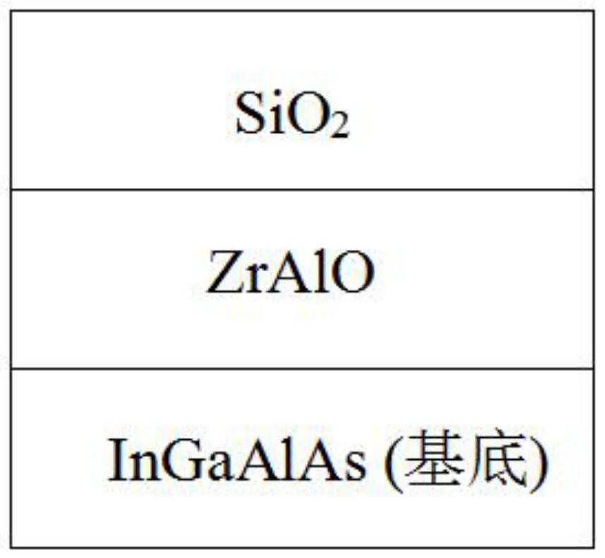
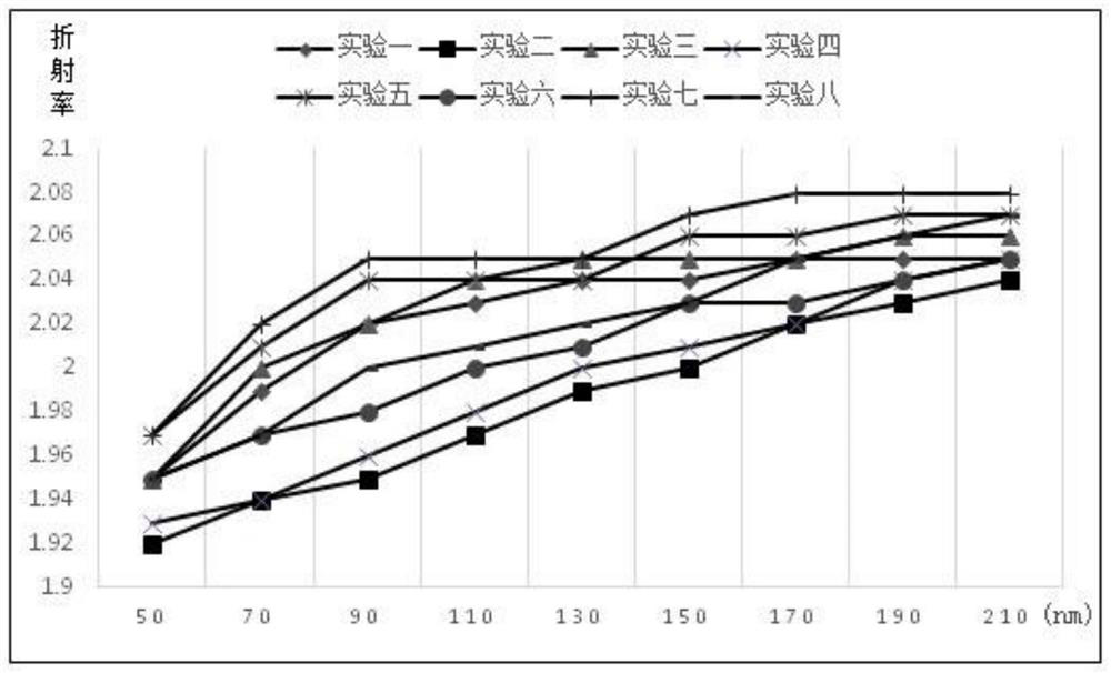
[0049] The following ZrAlO and ZrO 2 The above-mentioned process methods are used for coating under different temperature and film thickness conditions, that is, ZrAlO film coating is performed on the surface of the light cavity, and ZrO 2 The film is coated, and then the refractive index of the companion plate is tested using an ellipsometer.

[0050] Specifically, it is prepared in four groups:

[0051] 1) With the coating environment temperature as 160°C, the coating thickness (referring to ZrAlO film layer or ZrO 2 film thickness) are 50nm, 70nm, 90nm, 110nm, 130nm, 150nm, 170nm, 190nm, 210nm process conditions, using ZrAlO and ZrO 2 The film material is used for coating, and the accompanying sheet is placed with the furnace. Among them, ZrAlO is recorded as Experiment 1, and ZrO 2 Denoted as Experiment 2;

[0052] 2) The coating environment temperature is 180°C, and the coating thickness is 50nm, 70nm, 90nm, 110nm, 130nm, 150nm, 170nm, 190nm, 210nm process conditions,...

Embodiment 2

[0057] In this embodiment, the product is prepared according to the above-mentioned processing method, and the surface of the light exit cavity is coated with ZrAlO / SiO 2 Anti-reflection coating, coated with Al on the backlight 2 o 3 / Si / Al 2 o 3 The / Si film is a high-reflection film, and two Bar bars after the coating are randomly selected as the experimental group; the surface of the optical cavity is coated with ZrO 2 / SiO 2 Anti-reflection coating, coated with Al on the backlight 2 o 3 / Si / Al 2 o 3 The / Si film is a high-reflection film, and two Bar bars after coating are randomly selected as the control group. The experimental group and the control group are the same except for the anti-reflection film on the surface of the light cavity, and the other processes are the same.

[0058] Put the sampled bars of the experimental group and the control group into the alloy furnace to heat up the alloy furnace rapidly and keep the temperature constant for a certain perio...

Embodiment 3

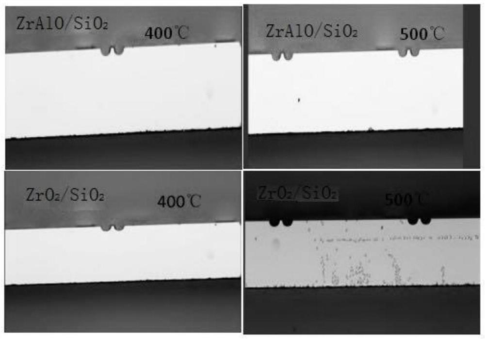
[0062] In this example, the SEM morphology detection of the product is carried out, and the product is prepared according to the above-mentioned processing method, and the surface of the light exit cavity is coated with ZrAlO / SiO 2 Anti-reflection coating, coated with Al on the backlight 2 o 3 / Si / Al 2 o 3 / Si film is a high-reflection film, randomly select 10pcs chips as the experimental group; the surface of the light cavity is coated with ZrO 2 / SiO 2 Anti-reflection coating, coated with Al on the backlight 2 o 3 / Si / Al 2 o 3 / Si film system high-reflection film, randomly select 10pcs chips as the control group; among them, the chips selected are tested and have normal appearance. The process methods are the same.

[0063] SEM morphology analysis was carried out on the light-emitting end and backlight end of the chips of the experimental group and the control group, as shown in the attached instructions. Figure 4 It can be seen from the appearance that the film s...


PUM


Abstract

The invention relates to the field of semiconductor lasers, in particular to a process method for processing a ZrAlO film system on a cavity surface of a semiconductor chip. The process method comprises the following steps: carrying out Bar strip cleavage and strip clamping on a product to be coated, quickly putting the product into evaporation coating equipment, vacuumizing, baking the product in a vacuum chamber, carrying out ion source pre-cleaning treatment on a cavity surface of the baked product, coating a ZrAlO / SiO2 film system antireflection film, carrying out ion source pre-cleaning treatment on a backlight surface of the product, and carrying out vacuum coating on the product to be coated with a ZrAlO / SiO2 film system antireflection film. Carrying out multi-layer high-reflection film system coating on the backlight surface of the product; wherein in the ZrO2 manufacturing process, 5-8% of Al is doped to prepare ZrAlO. The ZrAlO film layer structure has a stable tetragonal phase structure and has a stable refractive index under different film thicknesses and different temperatures, so that the failure of the laser caused by the defects of the film layer is avoided; meanwhile, compared with a conventional ZrO2 / SiO2 film system, ZrAlO effectively improves the stress between the film layers, and the situation that due to the fact that the stress of the film layers is too large at high temperature, the quality of the film layers becomes poor, and the performance of the laser is affected is avoided.

Description

technical field [0001] The invention relates to the field of semiconductor lasers, in particular to a process method for processing a ZrAlO film system on the cavity surface of a semiconductor chip. Background technique [0002] In the manufacturing process of semiconductor lasers, especially for DFB (Distributed Feedback Laser) lasers, the last step of the process needs to coat the cavity surface of the laser to realize the protection of the cavity surface, and by changing the emissivity of the cavity surface, it is realized for The gain effect of the laser output and the monitoring of the backlight; in addition, the quality of the cavity film layer also directly affects the service life and reliability of the laser. How to design a more reasonable film system and achieve excellent film quality has always been an industry practitioner At the same time, because the current high-speed chip solutions are generally made of Al-containing substrates (ie InGaAlAs) to improve the h...

Claims


Application Information

Patent Timeline
IPC IPC(8): C23C14/02C23C14/08C23C14/10C23C14/24H01S5/028
CPCC23C14/02C23C14/08C23C14/24C23C14/10H01S5/028
Inventor 赵军游顺青陈锋
Owner WUHAN GUANGANLUN OPTOELECTRONICS TECH CO LTD
Why Eureka
Try Eureka