

Sensitized fluorescent organic light-emitting device and application thereof
A sensitized fluorescence and luminescence technology, applied in the semiconductor field, can solve the problems of unreasonable, immature material collocation, low device performance, etc., and achieve the effects of improving efficiency, reducing injection barrier difference, and reducing device voltage
- Summary
- Abstract
- Description
- Claims
- Application Information
AI Technical Summary
Problems solved by technology
Method used
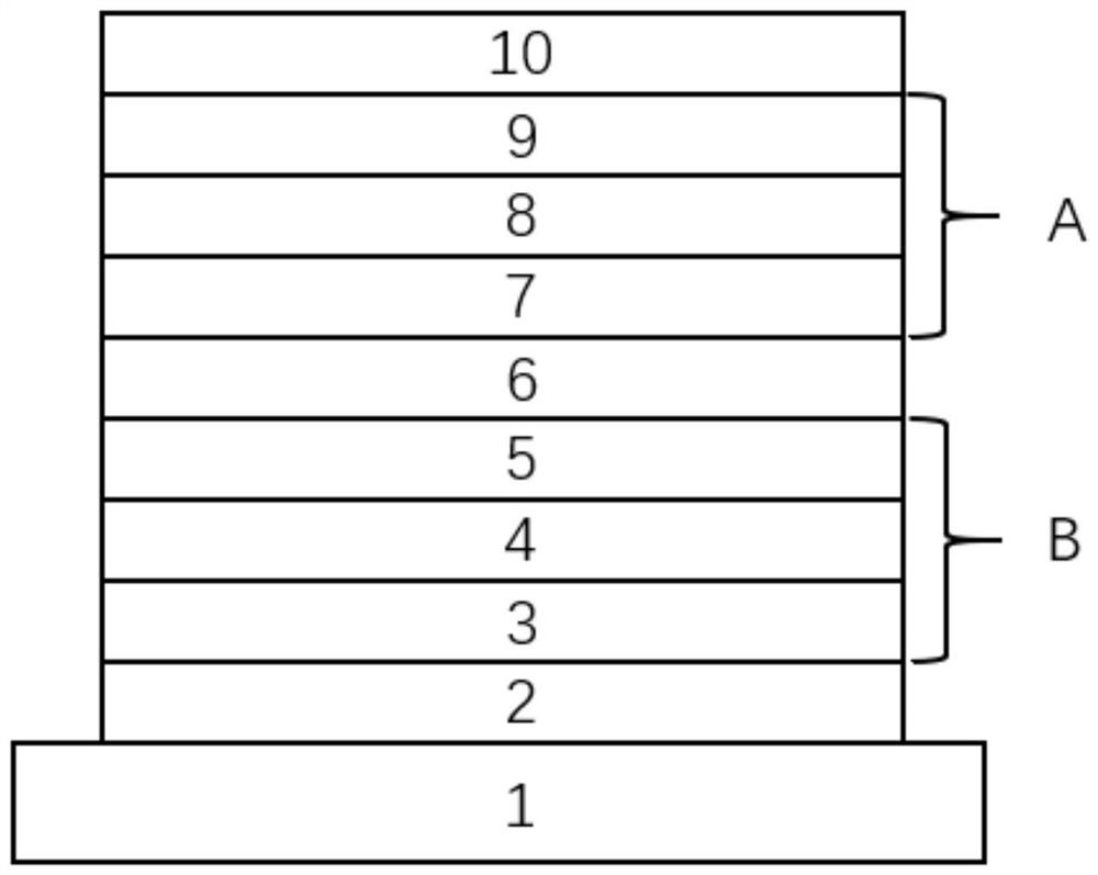
Image

Examples
Embodiment 1
[0173] Synthesis of compound EB1:
[0174]
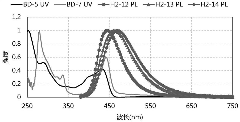
[0175] In a 250ml three-neck flask, under the protection of nitrogen, add 0.01mol raw material 1-1, 0.012mol raw material 2-1, 150ml toluene and stir to mix, then add 5×10 -5 mol Pd 2 (dba) 3 (Tris(dibenzylideneacetone)dipalladium), 5×10 -5molP(t-Bu) 3 , 0.03mol sodium tert-butoxide, heated to 105 ° C, refluxed for 24 hours, sampling point plate, showed no bromide (ie raw material 2-1) remaining, the reaction was complete; naturally cooled to room temperature, filtered, and the filtrate was rotary evaporated to no Fraction, through neutral silica gel column (mobile phase is petroleum ether: methylene chloride=1:2, volume ratio), obtains intermediate 1; HPLC purity 99.45%, yield 69.3%; Elemental analysis structure (molecular formula C 42 h 28 N 2 O): theoretical value C, 87.47; H, 4.89; N, 4.86; found value: C, 87.45; H, 4.86; N, 4.83. MS (m / z) (M+): theoretical value 576.22, found value 576.27.
[0176]
[0177] In a 2...
Embodiment 2
[0179] Synthesis of compound H1-1:
[0180]
[0181] Add 0.01mol of raw material 5-1 and 0.012mol of raw material 4-1 to 150mL of toluene:ethanol=2:1 mixed solvent, add 0.02mol of potassium carbonate, add 0.0002mol of Pd(PPh 3 ) 4 , reacted at 110° C. for 24 hours under a nitrogen atmosphere, took a sample and spotted the plate, and after the reaction of the reactant was complete, cooled and filtered, the filtrate was rotary evaporated to remove the solvent, and the crude product was passed through a silica gel column (the mobile phase was petroleum ether: dichloromethane = 1:3, volume ratio), obtain target compound H1-1; HPLC purity 98.97%, yield 78.5%; Elemental analysis structure (molecular formula C 42 h 26 N 2 o 2 ): theoretical value C, 85.69; H, 4.35; N, 4.65; test value: C, 85.61; H, 4.39; N, 4.69. MS (m / z) (M+): theoretical value 602.20, found value 602.32.
Embodiment 3
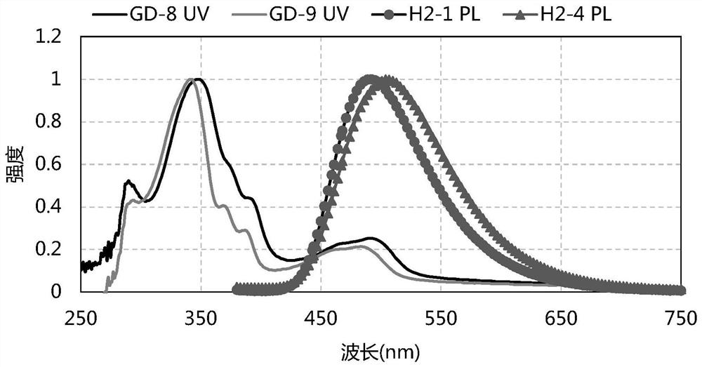
[0183] Synthesis of compound GD-12:
[0184]
[0185] In the three-necked flask, under the protection of nitrogen, add 0.01mol raw material 6-1, 0.025mol raw material 7-1, 150ml toluene and stir to mix, then add 5×10 -5 mol Pd 2 (dba) 3 , 5×10 -5 mol P(t-Bu) 3 , 0.03mol sodium tert-butoxide, heated to 105 ° C, reflux reaction for 16 hours, sampling point plate, showed no bromide (ie raw material 6-1) remaining, the reaction was complete; naturally cooled to room temperature, filtered, and the filtrate was rotary evaporated to nothing The fraction was passed through a neutral silica gel column (mobile phase: petroleum ether:dichloromethane=1:1, volume ratio) to obtain intermediate 2.
[0186] Under nitrogen atmosphere, add 0.01mol of intermediate 2 to the three-necked flask, then add 150ml of tert-butylbenzene to dissolve it, cool down to 0°C and keep it, slowly add 0.03mol of tert-butyllithium in pentane solution of 20ml, and then raise the temperature successively Rea...
PUM
| Property | Measurement | Unit |
|---|---|---|
| Thickness | aaaaa | aaaaa |
Abstract
Description
Claims
Application Information