High-efficiency crystalline silicon cell

A technology of crystalline silicon battery and crystalline silicon, which is applied in the direction of circuits, crystal growth, electrical components, etc., can solve the problems of affecting the effect of current derivation, large ohmic resistance, etc., achieve good passivation, reduce resistance, and improve cleanliness Effect

Pending Publication Date: 2022-04-19
江苏科来材料科技有限公司
View PDF13 Cites 0 Cited by
  • Summary
  • Abstract
  • Description
  • Claims
  • Application Information

AI Technical Summary

Problems solved by technology

However, in the conventional technology, the ohmic resistance of the contact between the electrode and the battery is relatively large, which will directly affect the derivation effect of the current

Method used


Image

  • High-efficiency crystalline silicon cell
  • High-efficiency crystalline silicon cell

Examples


preparation example 1

[0045] Preparation Example 1: This preparation example provides a cleaning agent for cleaning P-type silicon wafers, which is prepared by stirring and dissolving components in the following mass ratios:

[0046] Potassium hydroxide: sodium silicate: potassium hydrogen phosphate: lauryl polyoxyethylene ether: deionized water = 5:6:1:7:100.

preparation example 2

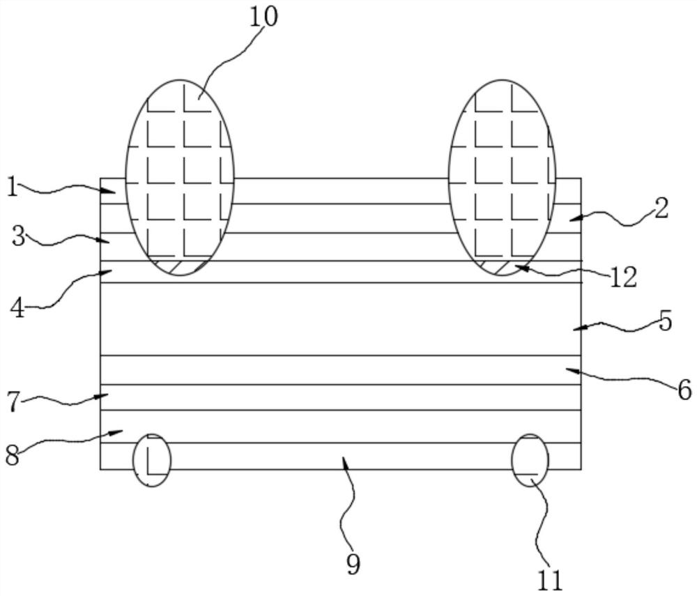
[0047] Preparation Example 2: A P-type heavily doped emitter 12 provided in this preparation example is prepared by the following steps:

[0048] A1-1 Clean the P-type silicon wafer by RCA cleaning method for 30 minutes, then place the cleaned P-type silicon wafer in the deposition chamber, and then place the heating furnace cover on the deposition chamber, and raise the temperature until the P-type silicon wafer reaches 770°C;

[0049] A1-2 evacuate the deposition chamber to a vacuum through a vacuum pump, then pass nitrogen gas into the vacuum deposition chamber, repeat five times;

[0050] A1-3 performs ion nitriding treatment on the surface of the P-type silicon wafer through a DC pulse power supply with an average current of 3000A and a maximum peak current of 10000A;

[0051] A1-4 feeds phosphorus trioxide and oxygen into the deposition chamber, the flow of phosphorus trioxide is controlled at 600 sccm, and the flow of oxygen is controlled at 400 sccm for 7 minutes until...

preparation example 3

[0057] Preparation example 3: the difference between this preparation example and preparation example 2 is that this preparation example uses the cleaning agent prepared in preparation example 1 to clean the P-type silicon wafer for 30 minutes.


PUM

PropertyMeasurementUnit
thicknessaaaaaaaaaa
electrical resistivityaaaaaaaaaa
thicknessaaaaaaaaaa

Abstract

The invention discloses a high-efficiency crystalline silicon cell, and relates to the technical field of homogeneous cells, the high-efficiency crystalline silicon cell comprises an N-type single crystal substrate, one side of the N-type single crystal substrate is provided with a P-type crystalline silicon diffusion layer, one side, deviating from the N-type single crystal substrate, of the P-type crystalline silicon diffusion layer is provided with a passivation part, one side, deviating from the P-type crystalline silicon diffusion layer, of the passivation part is provided with a first antireflection film, and the first antireflection film is provided with a second antireflection film. The first antireflection film is connected with a first electrode, the end, close to the N-type single crystal substrate, of the first electrode extends to make contact with the P-type crystalline silicon diffusion layer, P-type heavy doping treatment is conducted on an emitting electrode of the first electrode, and the N-type single crystal substrate is provided with a connecting part away from the P-type crystalline silicon diffusion layer. A second antireflection film is arranged on the side, away from the N-type single crystal substrate, of the connecting part, and a second electrode is connected to the second antireflection film. High doping treatment is performed on the first electrode, so that resistance of ohmic contact when the electrode is in contact with the battery can be reduced, and collection of current and export of current at the electrode position are facilitated.

Description

technical field [0001] The present application belongs to the technical field of batteries, and in particular relates to a high-efficiency crystalline silicon battery. Background technique [0002] Crystalline silicon cells, commonly known as solar cells, are an environmentally friendly energy conversion method. As human beings pay more and more attention to the environment, the power generation method mainly relying on thermal power will gradually leave the stage of history. Therefore, in recent years, the research on crystalline silicon cells has been deepened. [0003] The main substrate of the crystalline silicon battery is an N-type silicon layer and a P-type silicon layer. The N-type silicon layer and the P-type silicon layer will contact each other and form an interface, thereby forming a PN junction, and an internal electric field will be formed in the PN junction. At this time, the free electrons and holes excited by the absorption of photons near the interface wil...

Claims


Application Information

Patent Timeline
Patent Type & Authority Applications(China)
IPC IPC(8): H01L31/0216H01L31/18C11D1/72C11D3/04C11D3/06C11D3/08C11D3/60C30B31/02C30B33/00C30B29/06
CPCH01L31/02168H01L31/1868C11D1/72C11D3/08C11D3/044C11D3/06C30B31/02C30B33/00C30B29/06
Inventor 朱英明曹育娟孟祥国胡磊振邱凯坤
Owner 江苏科来材料科技有限公司
Why Eureka
Try Eureka