Monolithic integrated GaN/Ga2O3 Cascode enhanced anti-single event burnout device and preparation method thereof

A monolithic integration and anti-single event technology, which is applied in semiconductor/solid-state device manufacturing, semiconductor devices, electric solid-state devices, etc., can solve the problems of low devices and low threshold voltage, and achieve the effect of increasing threshold voltage and increasing reliability

Pending Publication Date: 2022-06-03
XIDIAN UNIV +2
View PDF0 Cites 2 Cited by
  • Summary
  • Abstract
  • Description
  • Claims
  • Application Information

AI Technical Summary

Problems solved by technology

Although the single-event burn-out of the third-generation wide-bandgap devices has a certain research status, the current single-event burn-out threshold voltage of all material devices is very low, and it is far lower than the breakdown voltage of the device itself, and there are serious reliability problems. , there is an urgent need to develop new transistor structures with enhanced anti-single event burnout characteristics

Method used


Image

  • Monolithic integrated GaN/Ga2O3 Cascode enhanced anti-single event burnout device and preparation method thereof
  • Monolithic integrated GaN/Ga2O3 Cascode enhanced anti-single event burnout device and preparation method thereof

Examples


preparation example Construction

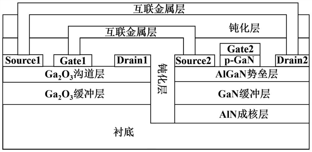
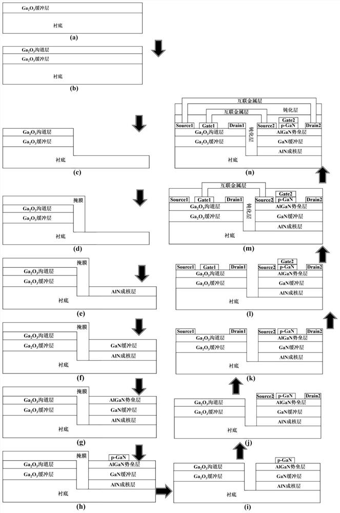
[0041] figure 2 This is the flow chart of the present invention to make a Cascode structure enhanced power device. As shown in the figure, a monolithic integrated GaN / Ga 2 O 3 The preparation method of the Cascode-enhanced anti-single particle burnout device comprises the following steps:

[0042] (1) The substrate surface is cleaned and pretreated to eliminate surface dangling bonds, and in H 2 Heat treatment at a temperature of 900℃-1200℃ in the atmosphere reaction chamber to remove surface contaminants;

[0043] (2) After the heat treatment, the substrate is deposited with a thickness of 100nm-1000nm by MOCVD process. 2 O 3 , as Ga 2 O 3 Buffer layer of FET structure;

[0044] (3) in Ga 2 O 3 On the buffer layer, MOCVD process is used to deposit Ga with a thickness of 100nm-1000nm 2 O 3 , as the channel layer of the device, and the doping concentration is 1 × 10 15 cm -3 -1×10 20 cm -3 Si;

[0045] (4) in Ga 2 O 3 A mask layer is grown on the channel laye...

Embodiment 1

[0061] Made with gallium oxide Ga 2 O 3 is the substrate, and Ga 2 O 3 Monolithically integrated GaN / Ga with 500nm FET channel layer thickness 2 O 3 Cascode Enhanced Anti-Single Event Burnout Device.

[0062] Step 1, to GaO 2 O 3 The substrate surface is pretreated to eliminate dangling bonds.

[0063] 1.1) The gallium oxide Ga 2 O 3 The substrate was soaked in HF acid solution for 1 min, and then placed in acetone solution, absolute ethanol solution and deionized water for ultrasonic cleaning for 10 min each, and the cleaned gallium oxide Ga 2 O 3 The substrate was blown dry with nitrogen;

[0064] 1.2) In H 2 The cleaned and blown-dried substrates are heat treated at a temperature of 1000°C in an atmosphere reaction chamber to remove surface contaminants.

[0065] Step 2, Make Ga 2 O 3 The buffer layer.

[0066] The preprocessed Ga 2 O 3 The substrate was placed in a metal organic chemical vapor deposition MOCVD system, the pressure of the reaction chamber...

Embodiment 2

[0096] Fabricated with sapphire as substrate, and Ga 2 O 3 Monolithically integrated GaN / Ga with 300nm FET channel layer thickness 2 O 3 Cascode Enhanced Anti-Single Event Burnout Device.

[0097] In step 1, the surface of the sapphire substrate is pretreated to eliminate dangling bonds.

[0098] 1.1) Put the sapphire substrate into the HF acid solution and soak it for 1 min, then put it into acetone solution, absolute ethanol solution and deionized water for ultrasonic cleaning for 10 min each, and dry the cleaned sapphire substrate with nitrogen gas;

[0099] 1.2) In H 2 The cleaned and blown-dried substrates are heat treated at a temperature of 1000°C in an atmosphere reaction chamber to remove surface contaminants.

[0100] Step 2, make Ga 2 O 3 The buffer layer.

[0101] Put the pretreated sapphire substrate into the metal organic chemical vapor deposition MOCVD system, set the pressure of the reaction chamber to 30 Torr and the temperature to 900 ° C; at the sam...


PUM

PropertyMeasurementUnit
thicknessaaaaaaaaaa
thicknessaaaaaaaaaa

Abstract

The invention discloses a monolithic integrated GaN / Ga2O3 Cascode enhanced anti-single event burnout device, which comprises a Ga2O3FET (Field Effect Transistor) structure and a GaN HEMT (High Electron Mobility Transistor) structure arranged on the right side of the Ga2O3FET structure, the Ga2O3FET structure and the GaN HEMT structure are arranged on a substrate, and a first passivation layer is arranged between the GaN HEMT structure and the Ga2O3FET structure; the Ga2O3 FET structure sequentially comprises a Ga2O3 buffer layer and a Ga2O3 channel layer from bottom to top, and a first source electrode, a first grid electrode and a first drain electrode are sequentially arranged above the Ga2O3 channel layer from left to right; the GaN HEMT structure sequentially comprises an AlN nucleating layer, a GaN buffer layer and an AlGaN barrier layer from bottom to top, a second source electrode, a p-GaN layer and a second drain electrode are sequentially arranged above the AlGaN barrier layer from left to right, and a second grid electrode is arranged above the p-GaN layer. By adopting the structure, a novel Ga2O3 enhanced device is realized, the weight and the complexity of an aerospace system are reduced, the reliability of the device is improved, and the single-particle burning threshold voltage of the device applied to an aerospace irradiation environment is improved.

Description

technical field [0001] The invention relates to the technical field of semiconductor devices, in particular to a monolithic integrated GaN / Ga 2 O 3 Cascode-enhanced anti-single particle burnout device and preparation method thereof. Background technique [0002] Semiconductor devices with high power density and high energy conversion are used in electrical power conversion of power electronic systems in aerospace, circuit control under high voltage and high current and other equipment. With the increasing energy consumption, the aerospace power supply system using hydraulic energy, gas energy and mechanical energy as energy has problems such as large volume, large fuel consumption and low energy conversion efficiency. Power devices with high power density and high reliability are the application development of a new type of power system that effectively promotes aerospace with electricity as the main environmental protection energy source. With the continuous update and d...

Claims


Application Information

Patent Timeline
Patent Type & Authority Applications(China)
IPC IPC(8): H01L27/085H01L21/8258
CPCH01L27/085H01L21/8258
Inventor 赵胜雷刘爽张进成舒磊赵杜钧李同德王亮赵元富郝跃
Owner XIDIAN UNIV
Why Eureka
Try Eureka