Light-emitting device and preparation method thereof

A light-emitting device, quantum dot light-emitting technology, applied in semiconductor/solid-state device manufacturing, semiconductor devices, electric solid-state devices, etc., can solve the problems of affecting electron injection efficiency, poor interface fusion, easy to form charges, etc., to reduce physical structure defects and surface roughness, good bonding tightness, and the effect of promoting regrowth

Pending Publication Date: 2022-07-01
TCL CORPORATION
View PDF0 Cites 0 Cited by
  • Summary
  • Abstract
  • Description
  • Claims
  • Application Information

AI Technical Summary

Problems solved by technology

[0004] The purpose of the present application is to provide a light-emitting device and its preparation method, aiming to solve the problem of poor interface fusion between the light-emitting layer and the electron transport layer, which affects the electron injection efficiency and is easy to form charge accumulation to a certain extent

Method used


Image

  • Light-emitting device and preparation method thereof
  • Light-emitting device and preparation method thereof
  • Light-emitting device and preparation method thereof

Examples


preparation example Construction

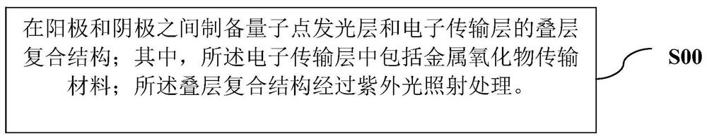
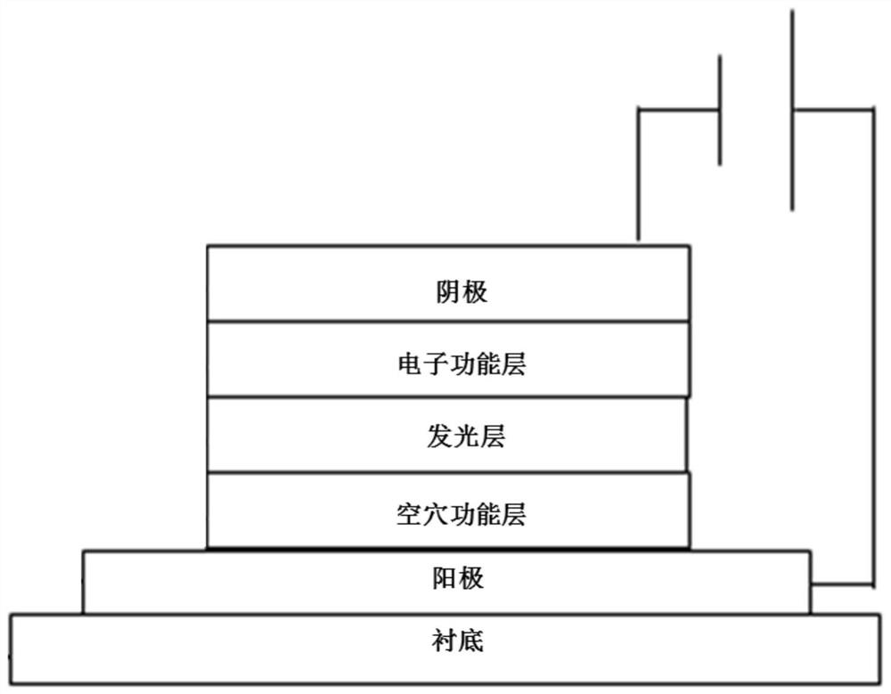
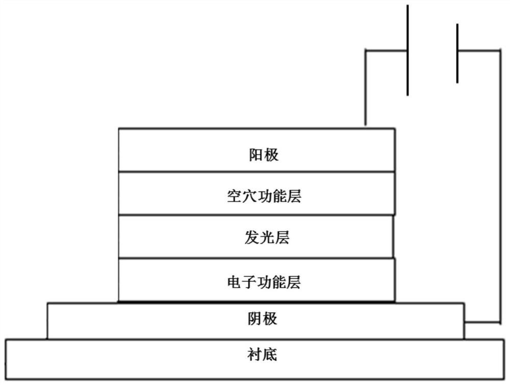
[0023] as attached figure 1 As shown, the first aspect of the embodiments of the present application provides a method for preparing a light-emitting device, including the following steps:

[0024] S00. A laminated composite structure of a quantum dot light-emitting layer and an electron transport layer is prepared between the anode and the cathode;

[0025] Wherein, the electron transport layer includes a metal oxide transport material; the laminated composite structure is treated by ultraviolet light irradiation.

[0026] In the method for preparing a light-emitting device provided in the first aspect of the present application, a laminated composite structure of a quantum dot light-emitting layer (QD) and an electron transport layer (ETL) is prepared between an anode and a cathode, and the laminated composite structure is irradiated with ultraviolet light ( UV) treatment, through ultraviolet light irradiation treatment, the electrons of O in the metal oxide transport mater...

Embodiment 1

[0072] A light-emitting diode, comprising the following preparation steps:

[0073] (1) Provide ITO anode, and pre-treat the anode: use alkaline washing solution (preferably PH>10 ultrasonic for 15 min, deionized water ultrasonic for 15 min twice, isopropanol ultrasonic cleaning for 15 min, dry at 80 ℃ for 2 h, ozone ultraviolet Process for 15min.

[0074] (2) forming a hole injection layer on the anode of step (1): under an electric field, spin-coating the PEDOT:PSS solution on the anode, spin-coating at 5000 rpm for 40 s, and then annealing at 150° C. for 15 min to form a hole-injecting layer; wherein , the action direction of the electric field is perpendicular to the anode and towards the hole injection layer, and the electric field strength is 10 4 V / cm.

[0075] (3) Forming a hole transport layer on the hole injection layer: under an electric field, spin-coat TFB solution (concentration of 8 mg / mL, solvent is chlorobenzene) on the hole injection layer, spin at 3000 rpm...

Embodiment 2

[0081] A light-emitting diode, comprising the following preparation steps:

[0082](1) Prepare the quantum dot light-emitting layer on the substrate: take the CdSe / ZnS quantum dot solution (concentration is 30mg / mL, the solvent is n-octane), put the CdSe / ZnS quantum dot solution in a glove box (water oxygen content is less than 0.1ppm) ) was spin-coated on the substrate at a speed of 3000 rpm to form a light-emitting layer.

[0083] (2) Preparation of electron transport layer in the light-emitting layer: in the glove box (water oxygen content is less than 0.1ppm), spin-coat ZnO solution (concentration is 45mg / mL, solvent is ethanol) on the light-emitting layer, spin-coating at 3000rpm for 30s Annealed at 80°C for 30min to form an electron transport layer.

[0084] (3) in H 2 The O content is less than 1ppm, the temperature is 80℃, the UV wavelength is 320nm, and the intensity is 300mJ / cm 2 UV light was applied to the laminated composite structure of the quantum dot light-em...


PUM

PropertyMeasurementUnit
particle diameteraaaaaaaaaa
wavelengthaaaaaaaaaa
thicknessaaaaaaaaaa

Abstract

The invention belongs to the technical field of display equipment, and particularly relates to a preparation method of a light-emitting device, which comprises the following steps: preparing a laminated composite structure of a quantum dot light-emitting layer and an electron transport layer between an anode and a cathode; wherein the electron transport layer comprises a metal oxide transport material; and the laminated composite structure is subjected to ultraviolet irradiation treatment. According to the preparation method of the light-emitting device, the laminated composite structure of the QD-ETL is prepared between the anode and the cathode, the laminated composite structure is subjected to ultraviolet irradiation treatment, electrons of O in the metal oxide transmission material are excited to form a complex with active metal elements such as Zn in the quantum dot light-emitting layer, and the quantum dot light-emitting layer is formed. The internal physical structure defect and the surface roughness of the electron transport layer are reduced, the electron transport migration efficiency is high, the interface combination of the quantum dot light-emitting layer and the electron transport layer is tight, the electron injection efficiency is high, QD-ETL interface charge accumulation is avoided, the device stability is good, and the service life is long.

Description

technical field [0001] The present application belongs to the technical field of display devices, and in particular, relates to a light-emitting device and a preparation method thereof. Background technique [0002] Quantum dots are nanocrystalline particles with a radius smaller than or close to the Bohr exciton radius, and their size and diameter are generally between one. Quantum dots have quantum confinement effect and can emit fluorescence when excited. Moreover, quantum dots have unique luminescence characteristics such as wide excitation peak, narrow emission peak, and tunable luminescence spectrum, which make quantum dot materials have broad application prospects in the field of optoelectronic luminescence. Quantum dot light-emitting diode (QLED) is a new type of display technology that has emerged rapidly in recent years. Quantum dot light-emitting diode is a device that uses colloidal quantum dots as the light-emitting layer. The quantum dot light-emitting layer i...

Claims


Application Information

Patent Timeline
Patent Type & Authority Applications(China)
IPC IPC(8): H01L51/50H01L51/54H01L51/56
CPCH10K71/40H10K50/115H10K50/16H10K2102/00H10K71/00H10K85/00H10K50/00
Inventor 王天锋
Owner TCL CORPORATION
Why Eureka
Try Eureka