Organic eutectic material and preparation method and application thereof
A eutectic material and organic technology, applied in the field of organic eutectic materials and their preparation, can solve the problems of cumbersome design structure and synthesis, affecting the application of semiconductor materials, hindering the rapid development of near-infrared phototransistors, and achieving low cost and crystallization The effect of good performance and good photoelectric performance
- Summary
- Abstract
- Description
- Claims
- Application Information
AI Technical Summary
Problems solved by technology
Method used
Image


Examples
Embodiment 1
[0043] A preparation method of an organic eutectic material, comprising the following steps:
[0044] Dissolve the donor molecule and the acceptor molecule in the solvent to obtain a mixed solution. The ratio of the donor molecule to the acceptor molecule is 1:1 according to the amount of the substance. The mixed solution is heated to 80°C with a heating table and heated. The temperature was kept constant for 3 hours until the donor molecule and the acceptor molecule were completely dissolved in the solvent, and the heating was stopped. Pipette 30 microliters of the mixed solution and add it dropwise to the silica side of the OTS-modified silicon wafer. The solvent is evaporated at room temperature of 20-25°C, and the thickness of 30-35nm is obtained on the silica side of the OTS-modified silicon wafer. The rod-shaped organic eutectic material, wherein the solvent is acetonitrile, and the concentration of the mixed solution is 1 mg / mL.
[0045] The donor molecule is 5,7-dihyd...
Embodiment 2
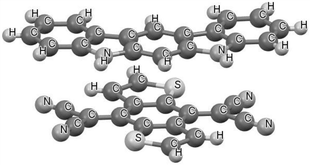
[0051] The organic eutectic material prepared in Example 1 is as follows figure 1 shown, which is 5,7-dihydro-indolo[2,3-B]carbazole-2,2'-(benzo[1,2-B:4,5-B']dithiophene- 4,8-Disubunit) Dimalononitrile (5,7-ICZ—DTTCNQ), organic eutectic material is formed by the self-assembly non-covalent bond of donor molecule and acceptor molecule, wherein, according to the amount of substance In parts, the ratio of donor molecules to acceptor molecules in the organic eutectic material is 1:1.
[0052] From single crystal X-ray diffraction analysis, it is concluded that the organic eutectic material is monoclinic, and the space group is C 1 2 / c 1 , the unit cell parameters of the organic eutectic material are: a=39.0513(7), b=7.11710(10), c=19.8653(3), α=90, β=90.130(2), γ=90.
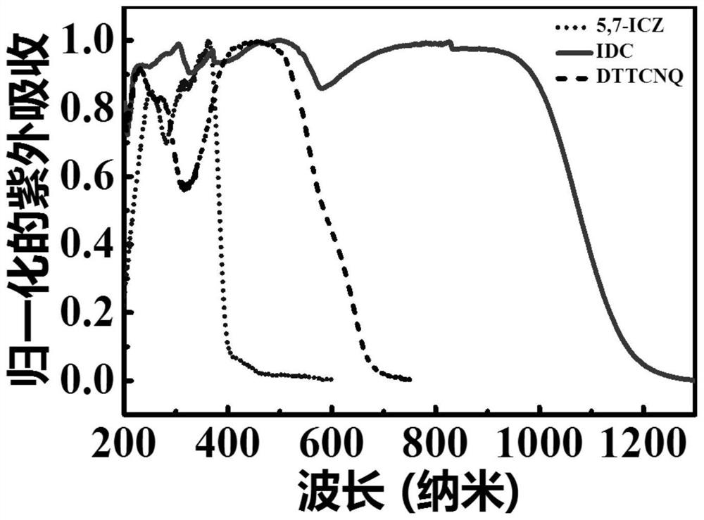
[0053] figure 2 for 5,7-ICZ, DTTCNQ, and 5,7-ICZ—DTTCNQ ( figure 2 IDC) UV-Vis absorption spectrum in the solid state. Depend on figure 2It can be seen that the maximum absorption sideband peak of the orga...
Embodiment 3
[0055] In the application of the organic eutectic material in the field effect transistor in Example 1, the organic eutectic material is used as the organic semiconductor layer (active layer) in the field effect transistor. Field effect transistor structure such as image 3 As shown, the silicon layer in the OTS-modified silicon wafer is the gate electrode, the silicon dioxide layer of the OTS-modified silicon wafer is an insulating layer, and the insulating layer is an organic semiconductor layer ( image 3 The eutectic in the organic semiconductor layer is the source electrode and the drain electrode.
[0056] The method of preparing the source electrode and the drain electrode: paste a copper mesh as a mask on the OTS modified silicon wafer, and the vacuum degree is 10 in the evaporation chamber. -6 Under the conditions of torr and rate of 0.1 nm / s, gold was vapor-deposited on OTS-modified silicon wafers as source and drain electrodes (both with an aspect ratio of 8:1), an...
PUM
| Property | Measurement | Unit |
|---|---|---|
| Length | aaaaa | aaaaa |
Abstract
Description
Claims
Application Information
 - Generate Ideas
- Intellectual Property
- Life Sciences
- Materials
- Tech Scout
- Unparalleled Data Quality
- Higher Quality Content
- 60% Fewer Hallucinations
Browse by: Latest US Patents, China's latest patents, Technical Efficacy Thesaurus, Application Domain, Technology Topic, Popular Technical Reports.
© 2025 PatSnap. All rights reserved.Legal|Privacy policy|Modern Slavery Act Transparency Statement|Sitemap|About US| Contact US: help@patsnap.com