Manufacturing method of quantum dot laser

A production method and quantum dot technology, applied in the direction of lasers, phonon exciters, semiconductor lasers, etc., can solve problems such as the inability to prepare high-quality p-GaN layers, and achieve low cost, fast growth rate, and high preparation quality. Effect

Active Publication Date: 2022-07-08
SUZHOU INST OF NANO TECH & NANO BIONICS CHINESE ACEDEMY OF SCI
View PDF4 Cites 0 Cited by
  • Summary
  • Abstract
  • Description
  • Claims
  • Application Information

AI Technical Summary

Problems solved by technology

[0005] The object of the present invention is to provide a method for manufacturing a quantum dot laser, which can overcome problems such as the inability to prepare high-quality p-GaN layers in the prior art

Method used


Image

  • Manufacturing method of quantum dot laser
  • Manufacturing method of quantum dot laser

Examples


Embodiment 1

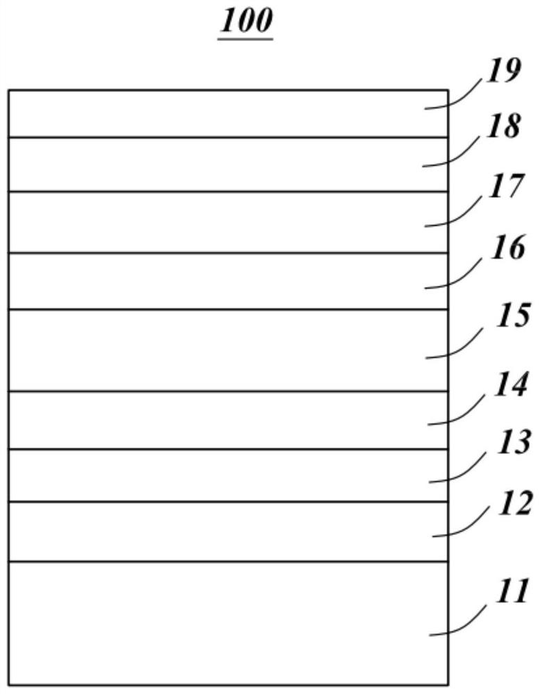
[0041] ginseng figure 1 As shown, the quantum dot laser 100 includes a substrate 11, a buffer layer 12, an n-type confinement layer 13, an n-type waveguide layer 14, a quantum dot active region 15, a p-type waveguide layer 16, an electron confinement layer 17, and a p-type confinement layer. 18 and p-type contact layer 19.

[0042] The substrate 11 is a sapphire substrate or a Si substrate; the buffer layer 12 is doped n-GaN with a thickness of 5 μm, using Si as a dopant, and the doping concentration is greater than or equal to 2×10 18 cm -2 ; The n-type confinement layer 13 is a plurality of periods of Al 0.15 GaN 0.85 / GaN, the overall thickness is 1000nm, the number of cycles is 200, Si is used as a dopant, and the doping concentration is greater than or equal to 2×10 18 cm -2 ; n-type waveguide layer 14 is In 0.05 Ga 0.95 N, the thickness is 100nm, Si is used as the dopant, and the doping concentration is greater than or equal to 1×10 18 cm -2 ; The quantum dot ac...

Embodiment 2

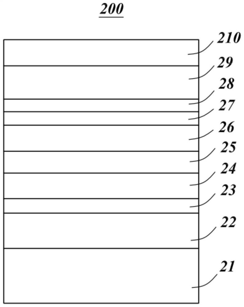
[0048] ginseng figure 2 As shown, quantum dot laser 200 includes substrate 21, n-type confinement layer 22, n-type spacer layer 23, n-type waveguide layer 24, quantum dot active region 25, p-type waveguide layer 26, p-type spacer layer 27, electrons Confinement layer 28 , p-type confinement layer 29 and p-type contact layer 210 .

[0049] The substrate 21 is an n-type GaN self-supporting substrate; the n-type confinement layer 22 is a plurality of cycles of Al 0.15 GaN 0.85 / GaN, Al 0.15 GaN 0.85 The thickness of the layer is 2.5nm, the thickness of the GaN layer is 2.5nm, and the number of cycles is 200. Si is used as a dopant, and the doping concentration is greater than or equal to 2×10 18 cm -2 ; The thickness of the n-type GaN spacer layer 23 is 10 nm. Si is used as a dopant, and the doping concentration is greater than or equal to 1×10 18 cm -2 ; n-type waveguide layer 24 is In 0.05 Ga 0.95 N, the thickness is 120nm, Si is used as the dopant, and the doping co...


PUM

PropertyMeasurementUnit
thicknessaaaaaaaaaa
thicknessaaaaaaaaaa
thicknessaaaaaaaaaa

Abstract

The invention discloses a manufacturing method of a quantum dot laser, which comprises the following steps: in MOCVD (Metal Organic Chemical Vapor Deposition) equipment, sequentially growing an n-type limiting layer and an n-type waveguide layer on a substrate to obtain a preliminary sample; and transferring the preliminary sample to MBE equipment, and then sequentially growing a quantum dot active region, a p-type waveguide layer, an electron limiting layer, a p-type limiting layer and a p-type contact layer on the n-type waveguide layer. The GaN-based quantum dot laser has the advantages that the MOCVD process is low in cost and high in growth rate, and the MBE process is good in low-dimensional material growth and is prepared on p-GaN, so that the prepared GaN-based quantum dot laser has the characteristics of high-temperature stability, low threshold current density and the like.

Description

technical field [0001] The present invention relates to the technical field of semiconductor devices, in particular to a manufacturing method of a quantum dot laser. Background technique [0002] Following the first and second generation semiconductors, gallium nitride (GaN)-based semiconductor materials, known as the third generation wide bandgap semiconductor materials, have wide band gaps, high thermal conductivity, and large impact. The advantages of through electric field, high electron mobility, and as a direct bandgap luminescent material, have gradually entered the public's field of vision. Its members include indium nitride, gallium nitride and aluminum nitride and their alloy compounds. Through the control of components, the forbidden band width of quaternary alloy compounds at room temperature is continuously adjustable in the range of 0.7eV ~ 6.2eV, which can cover the visible light band, so it has a wide range of applications in the field of optoelectronic devi...

Claims


Application Information

Patent Timeline
Patent Type & Authority Applications(China)
IPC IPC(8): H01S5/34H01S5/343C30B29/68C30B29/40C30B25/18C30B25/02
CPCH01S5/3412H01S5/34333C30B29/403C30B29/406C30B29/68C30B25/02C30B25/18C30B25/183H01S2304/04H01S2304/02
Inventor 张鹏陆书龙杨文献顾颖邱海兵张雪
Owner SUZHOU INST OF NANO TECH & NANO BIONICS CHINESE ACEDEMY OF SCI
Why Eureka
Try Eureka