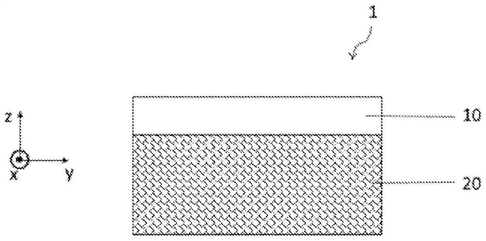
Method for producing composite structure comprising thin layer of monocrystalline SiC on carrier substrate of polycrystalline SiC
A carrier substrate and production method technology, applied in semiconductor/solid-state device manufacturing, electrical components, circuits, etc., can solve problems such as low density, no expansion defects, adverse effects on power device performance and reliability, etc.
- Summary
- Abstract
- Description
- Claims
- Application Information
AI Technical Summary
Problems solved by technology
Method used
Image

Examples
Embodiment 1
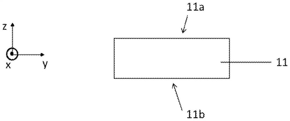
[0096] According to one non-limiting exemplary embodiment, the initial substrate 11 provided in step a) of the production method is a wafer made of c-SiC, which is the 4H polytype, relative to axis has an orientation of 4.0°±0.5° and has a diameter of 150 mm and a thickness of 350 μm.
[0097] Before step b) of the epitaxial growth of the c-SiC donor layer 110, a conventional RCA cleaning procedure (Standard Clean 1 + Standard Clean 2) is carried out on the initial substrate 11, followed by Caroline acid (sulfuric acid and hydrogen peroxide mixture), followed by HF (hydrofluoric acid).
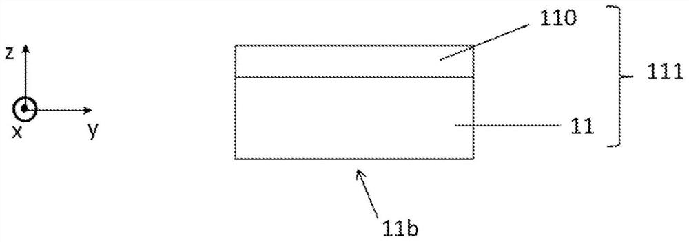
[0098] Growth using precursors such as monosilane (SiH4) and propane (C3H8) or ethylene (C2H4) in an epitaxial chamber at a temperature of 1650° C. produces a c-SiC donor layer 110 with a thickness of 30 μm (growth rate : 10 μm / hour). The BPD defect density of the donor layer is about 1 / cm 2 .
[0099] With 150keV energy and 6 E 16 H+ / cm 2 A dose of H ions is implanted through the free s...
Embodiment 2
[0106] According to one non-limiting exemplary embodiment, the initial substrate 11 provided in step a) of the production method is a wafer made of c-SiC, which is the 4H polytype, relative to axis has an orientation of 4.0°±0.5° and has a diameter of 150 mm and a thickness of 350 μm.
[0107] Before step b) of the epitaxial growth of the c-SiC donor layer 110, a conventional RCA cleaning procedure (Standard Clean 1 + Standard Clean 2) is carried out on the initial substrate 11, followed by Caroline acid (sulfuric acid and hydrogen peroxide mixture), followed by HF (hydrofluoric acid).
[0108] The conversion layer 13 is formed in the epitaxy chamber. Before starting the epitaxial growth of this layer 13 on the initial substrate 11, a hydrogen bake is carried out in the chamber at a temperature of 1700°C for a period of 10 to 20 minutes. Epitaxial growth of the conversion layer 13 of c-SiC is then carried out at a temperature of 1650°C using precursors such as monosilane (Si...
PUM
| Property | Measurement | Unit |
|---|---|---|
| Defect density | aaaaa | aaaaa |
Abstract
Description
Claims
Application Information
 - R&D Engineer
- R&D Manager
- IP Professional
- Industry Leading Data Capabilities
- Powerful AI technology
- Patent DNA Extraction
Browse by: Latest US Patents, China's latest patents, Technical Efficacy Thesaurus, Application Domain, Technology Topic.
© 2024 PatSnap. All rights reserved.Legal|Privacy policy|Modern Slavery Act Transparency Statement|Sitemap