
GaN-based light-emitting diode based on C-doped current expansion layer and preparation method of GaN-based light-emitting diode

A technology of light emitting diode and current expansion layer, applied in the field of microelectronics, can solve the problems of affecting the crystal quality of the light emitting quantum well layer, increase the complexity of the process, etc., and achieve the effects of alleviating the current congestion effect, high availability and simple process

Pending Publication Date: 2022-08-02
XIDIAN UNIV
View PDF0 Cites 0 Cited by
  • Summary
  • Abstract
  • Description
  • Claims
  • Application Information

AI Technical Summary

Problems solved by technology

[0004] However, these methods require additional growth steps, increasing process complexity, and the additional inserted layer structure may affect the crystal quality of the light-emitting quantum well layer

Method used


Image

  • GaN-based light-emitting diode based on C-doped current expansion layer and preparation method of GaN-based light-emitting diode
  • GaN-based light-emitting diode based on C-doped current expansion layer and preparation method of GaN-based light-emitting diode
  • GaN-based light-emitting diode based on C-doped current expansion layer and preparation method of GaN-based light-emitting diode

Examples


Embodiment 1

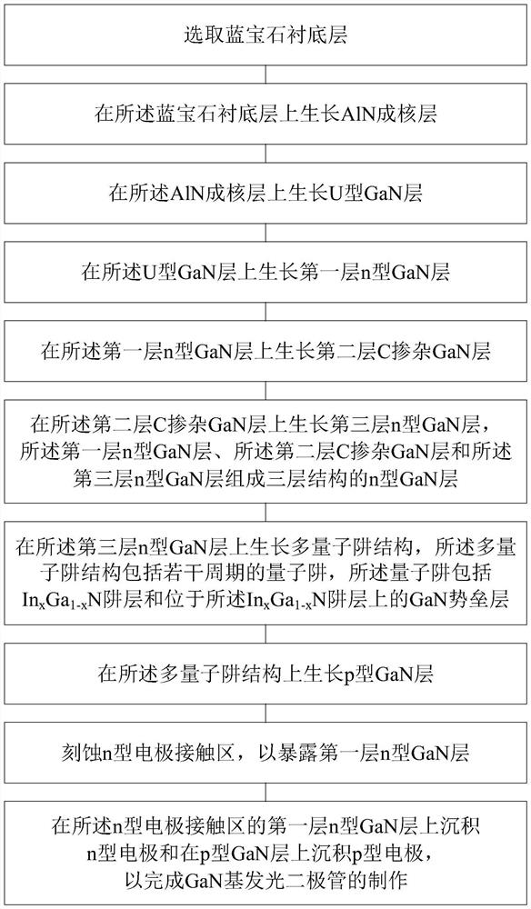
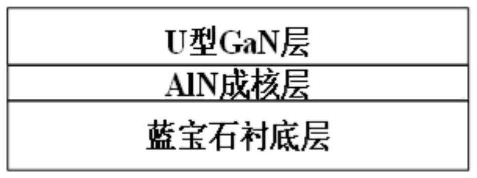
[0054] See figure 1 and Figure 2, figure 1A schematic flowchart of a preparation method of a GaN-based light-emitting diode based on a C-doped current spreading layer provided by an embodiment of the present invention, and FIG. 2 is a GaN-based light-emitting diode based on a C-doped current spreading layer provided by an embodiment of the present invention. Process schematic diagram of the fabrication method of the diode. The invention provides a preparation method of a GaN-based light-emitting diode based on a C-doped current spreading layer, and the preparation method of the GaN-based light-emitting diode comprises:

[0055] Step 1, see Figure 2a , select the sapphire substrate layer.

[0056] Step 1.1, cleaning the sapphire substrate layer.

[0057] Step 1.2, under the temperature condition of 900-1200°C, heat treatment for 5-10min on the sapphire substrate layer.

[0058] Specifically, it is placed in the MOCVD reaction chamber of metal organic chemical vapor deposi...

Embodiment 2

[0089] On the basis of Embodiment 1, the present invention also provides a preparation method of a C-doped blue LED with an emission wavelength of 450 nm, the preparation method comprising:

[0090] Step one, heat treatment.

[0091] After the sapphire substrate layer is cleaned, it is placed in the MOCVD reaction chamber, and the vacuum degree of the reaction chamber is reduced to 2×10 -2 Torr; then pass hydrogen into the reaction chamber, and under the condition that the pressure of the MOCVD reaction chamber reaches 20 Torr, the sapphire substrate layer is heated to a temperature of 900° C. and kept for 10 minutes to complete the heat treatment of the sapphire substrate layer.

[0092] Step 2, high temperature nitriding.

[0093] The heat-treated sapphire substrate layer was placed in a reaction chamber with a temperature of 1000° C., and ammonia gas with a flow rate of 3,500 sccm was introduced for nitridation for 5 minutes to complete the nitridation.

[0094] Step 3, g...

Embodiment 3

[0114] On the basis of the first embodiment, the present invention also provides a preparation method of a C-doped green LED with an emission wavelength of 520 nm, the preparation method comprising:

[0115] Step one, heat treatment.

[0116] After cleaning the sapphire substrate layer, it was placed in the MOCVD reaction chamber, and the vacuum degree of the reaction chamber was reduced to 2×10 -2 Torr; then pass hydrogen into the reaction chamber, and under the condition that the pressure of the MOCVD reaction chamber reaches 400 Torr, the sapphire substrate layer is heated to a temperature of 1000° C. and kept for 7 minutes to complete the heat treatment of the sapphire substrate layer.

[0117] Step 2, high temperature nitriding.

[0118] The heat-treated sapphire substrate layer was placed in a reaction chamber with a temperature of 1050° C., and ammonia gas with a flow rate of 3500 sccm was introduced into the nitridation for 4 minutes to complete the nitridation.

[0...


PUM

PropertyMeasurementUnit
thicknessaaaaaaaaaa
thicknessaaaaaaaaaa
thicknessaaaaaaaaaa

Abstract

The invention relates to a GaN-based light emitting diode based on a C-doped current expansion layer and a preparation method of the GaN-based light emitting diode. The method comprises the following steps: growing an AlN nucleating layer on a sapphire substrate layer; growing a U-shaped GaN layer on the AlN nucleating layer; growing a first n-type GaN layer on the U-type GaN layer; growing a second C-doped GaN layer on the first n-type GaN layer; growing a third n-type GaN layer on the second C-doped GaN layer; growing a multi-quantum well structure on the third n-type GaN layer; growing a p-type GaN layer on the multi-quantum well structure; etching the n-type electrode contact region to expose the first n-type GaN layer; and depositing an n-type electrode on the first n-type GaN layer of the n-type electrode contact region and depositing a p-type electrode on the p-type GaN layer to complete the manufacturing of the GaN-based light emitting diode. According to the preparation method of the GaN-based light-emitting diode based on C doping, a C-doped GaN layer is used as a current expansion layer, the performance and reliability of the LED are improved, the method is simple, and introduction of an additional growth source and process steps is not needed.

Description

technical field [0001] The invention belongs to the technical field of microelectronics, and relates to a GaN-based light-emitting diode based on a C-doped current spreading layer and a preparation method thereof. Background technique [0002] GaN-based light-emitting diodes (LEDs, Light-Emitting Diodes) have the advantages of high efficiency, energy saving, environmental protection, long life, small size, good color rendering and response speed, and LED-based semiconductor lighting has gradually replaced traditional lighting. [0003] Due to the price and size constraints of GaN single crystals, heteroepitaxy is usually used for the growth of GaN. Sapphire is the most commonly used substrate for GaN growth. It has the advantages of mature production technology, moderate price, high mechanical strength and high cost performance. However, since sapphire is an insulator, devices with vertical structures cannot be fabricated, and LEDs with lateral structures are currently the ...

Claims


Application Information

Patent Timeline
Patent Type & Authority Applications(China)
IPC IPC(8): H01L33/00H01L33/14
CPCH01L33/0075H01L33/0066H01L33/14
Inventor 许晟瑞彭若诗江青聪范晓萌苏华科张涛张雅超张进成郝跃
Owner XIDIAN UNIV
Learn More