Miniature colloid impeller and making method thereof
A technology of a propeller and a colloid, which is applied in the field of miniaturized colloid propeller and its manufacturing, can solve the problems of the large size and weight of the nozzle array, the large volume of the servo mechanism, and the inability to generate the colloid propeller, and achieves low manufacturing cost and high structure. Simple, Reliable Effects
- Summary
- Abstract
- Description
- Claims
- Application Information
AI Technical Summary
Problems solved by technology
Method used
Image
Examples
specific Embodiment approach
[0035] The micro-colloid propeller provided by the present invention is composed of a micro-spray head array, each of which includes a source electrode and an extraction electrode. The voltage applied between the extraction electrodes forms a high field strength at the top of the source electrode at the same time, and the high field strength induces the charge of the strong polar working fluid to form a liquid cone (CONE-JET), and finally breaks into charged droplets and is High field strength accelerates, forming thrust. Generally, a mixture of glycerin and sodium iodide (10:2 by weight) is used as the working medium.
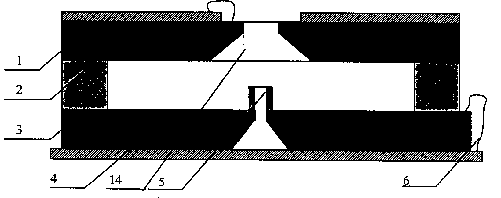
[0036] figure 1 It is the overall structure schematic diagram of the miniature colloid thruster of the present invention, among the figure 3 is the lower plate of the miniature colloid thruster, also referred to as the source silicon chip in the present invention, and the hollow columnar protrusion 5 on it is exactly the source, and the columnar source N pol...
Embodiment
[0058] 1. The manufacturing steps of the lower silicon wafer are:
[0059] (1) Deposit silicon dioxide and silicon nitride on both sides of the silicon wafer;
[0060] (2) Patterning the silicon dioxide and silicon nitride layers on the back of the silicon wafer to form a mask for bulk silicon etching;
[0061] (3) corroding liquid silicon with potassium hydroxide to corrode the silicon wafer by 240 microns;
[0062] (4) After rinsing, aluminum is steamed on the front side of the silicon wafer, and photolithography is performed;
[0063] (5) Using photoresist as a mask, dry-etching 80 microns by inductively coupled plasma (ICP) to form a hollow protruding inner cavity on the source electrode;
[0064] (6) Remove the photoresist, use patterned aluminum as a mask, and inductively coupled plasma (ICP) dry-etch 60 microns to form a hollow column of the source;
[0065] (7) Aluminum is sputtered on the front to form the conductive electrode of the source;
[0066] 2. The produc...
PUM
 Abstract
Description
Claims
Application Information


