

Distributed feedback semiconductor laser and electric absorption modulator integrated light source and mfg. method
A distributed feedback, semiconductor technology, used in semiconductor lasers, lasers, laser parts, etc., can solve the problems of inability to independently optimize lasers and modulators, difficult to achieve high-performance light source requirements, and difficult to reduce device manufacturing costs, and achieve low loss. , strong gain coupling coefficient, the effect of reducing junction capacitance
- Summary
- Abstract
- Description
- Claims
- Application Information
AI Technical Summary
Problems solved by technology
Method used
Image

Examples
Embodiment 1
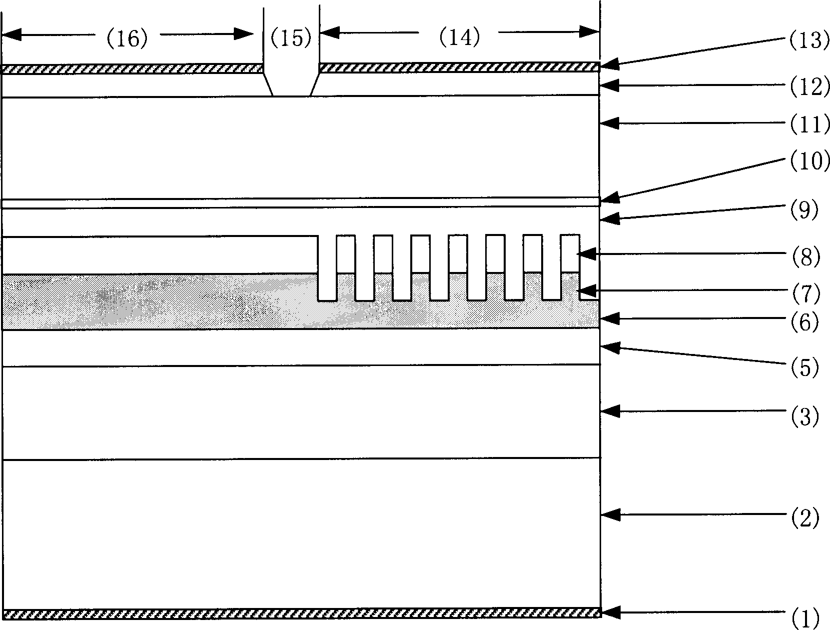
[0035] This embodiment introduces an InGaAsP DFB laser / EA modulator integrated laser device with an operating wavelength of 1550 nm based on a selective area epitaxy structure.
[0036] The epitaxial material structure of the device is as attached figure 1 As shown, among them: (1) N electrode, (2) substrate, (3) buffer layer, (5) lower waveguide layer, (6) multi-quantum well active layer, (7) grating, (8) upper waveguide layer, (9) leveling grating material, (10) etch stop layer, (11) upper confinement layer, (12) ohmic contact layer, (13) p-electrode, (14) DFB laser part, (15) electrode isolation part , (16) EA modulator part. The modulator and laser share a highly doped n-type InP substrate material. First grow an n-type InP buffer layer (thickness 160nm, doping concentration about 1×10 18 cm -3 ), non-doped lattice matching InGaAsP lower waveguide layer (thickness 80nm, light fluorescence wavelength 1150nm). Then make a layer of 200nm thick Si0 2 Mask, the gap width ...
Embodiment 2
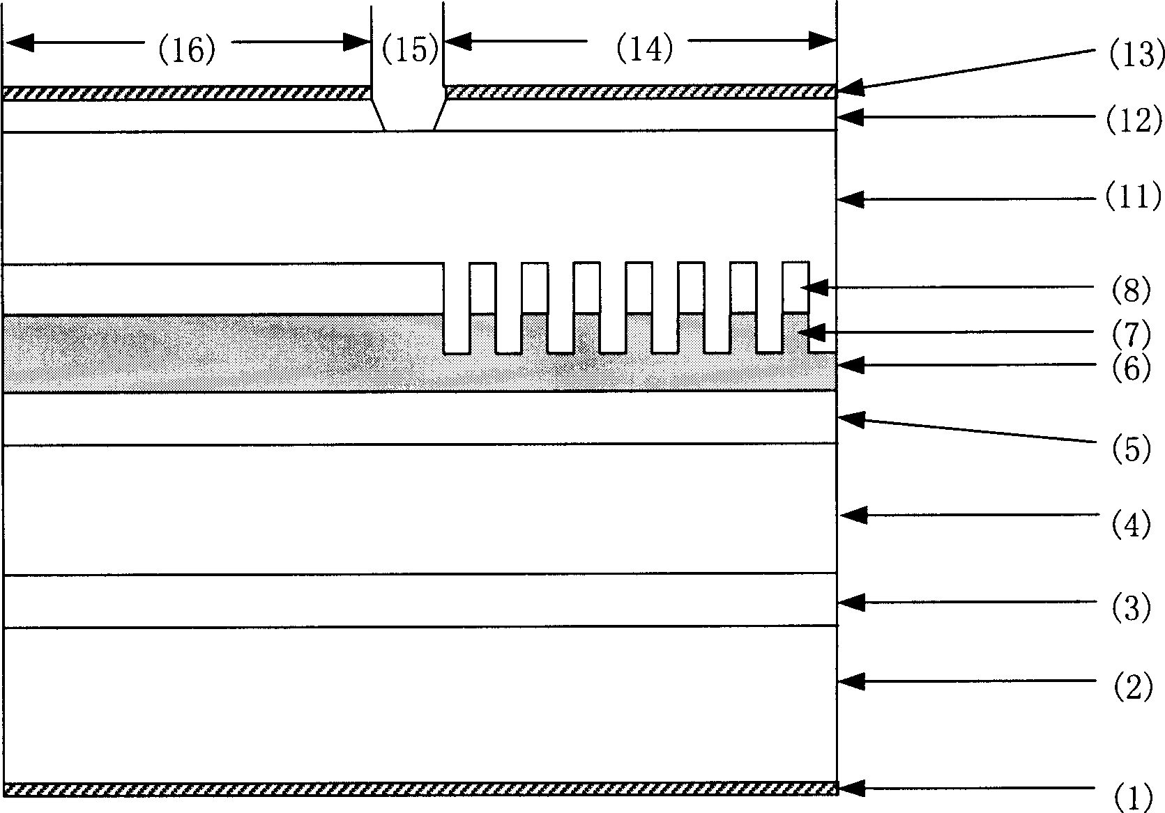
[0040] This embodiment introduces an InGaAlAs DFB laser / EA modulator integrated laser device with an operating wavelength of 1310 nm based on the same epitaxial layer structure.
[0041] The laser and modulator share a highly doped n-type InP substrate material. In the first epitaxy process first in n + -On the InP substrate, the n-InP buffer layer (thickness 500nm, doping concentration about 1×10) was sequentially grown by MOCVD 18 cm -3 ), non-doped lattice-matched InGaAsP lower waveguide layer (thickness 100nm, optical fluorescence wavelength 1050nm), non-doped strained InGaAlAs multi-quantum well active layer (10 periods, 1% compressive strain well, thickness 6nm; lattice-matched barrier , thickness 10nm, photofluorescence wavelength 1270nm), non-doped lattice matching InGaAsP upper waveguide layer (thickness 150nm, photofluorescence wavelength 1050nm). Then, for the laser part, 5 quantum wells are etched away by holographic exposure and dry etching to form a gain grati...
Embodiment 3
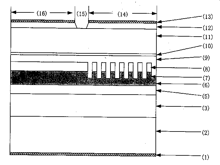
[0045] This embodiment introduces a GaAs / GaAlAs DFB laser / EA modulator integrated laser device with an operating wavelength of 850 nm based on quantum well partial disorder technology.
[0046] The epitaxial material structure of the device is as attached figure 2 As shown, among them: (1) N electrode, (2) substrate, (3) buffer layer, (4) lower confinement layer, (5) lower waveguide layer, (6) multi-quantum well active layer, (7) Grating, (8) upper waveguide layer, (11) upper confinement layer, (12) ohmic contact layer, (13) p-electrode, (14) DFB laser part, (15) electrode isolation part, (16) EA modulator part . The laser and modulator share a highly doped n-type GaAs substrate material. In the first epitaxial process, the n-GaAs buffer layer (thickness 500nm, doping concentration about 1×10 18 cm -3 ), undoped lattice-matched Ga 1-x al x As lower confinement layer (thickness 1000nm, x=0.45, doping concentration about 5×10 17 cm -3 ), undoped lattice-matched Ga 1-x ...
PUM
| Property | Measurement | Unit |
|---|---|---|
| Thickness | aaaaa | aaaaa |
| Wavelength | aaaaa | aaaaa |
| Doping concentration | aaaaa | aaaaa |
Abstract
Description
Claims
Application Information