

Method for preparing tw-dimension ordered nano ring, nano hole and nano self-assembling single layer film
A nano-self-assembly, nano-ring technology, used in nanostructure fabrication, nanotechnology, nanotechnology, etc.
- Summary
- Abstract
- Description
- Claims
- Application Information
AI Technical Summary
Problems solved by technology
Method used
Image

Examples
Embodiment 1
[0029]Under the protection of nitrogen, distilled water is used as a dispersion medium, and styrene and (meth)acrylic acid are used as monomers for soap-free emulsion polymerization to obtain an emulsion of stable monodisperse crosslinked polymer microspheres. For example: under the protection of nitrogen, using 100 ml of distilled water as the dispersion medium, 10 g of styrene, 0.5 g of 4,4'-dimethylacryloxy-2,2'-diphenylpropane, 1.2 g (Meth) acrylic acid, 0.08 g of potassium persulfate or ammonium persulfate, 0.24 g of sodium bicarbonate, were added to a reactor equipped with a mechanical stirrer and a reflux condenser, and the mechanical stirring speed was 300 rpm. The soap-free emulsion polymerization reaction is carried out in a water bath at 70°C. There is no need to add any surfactants and dispersants. After 24 hours of reaction, a stable milky white surface is obtained with a monodisperse cross-linked polymer with a negative charge and a rich surface. The emulsion of styr...
Embodiment 2
[0033] 1. Monodisperse polymer microspheres and silicon wafer treatment, and the preparation of three-dimensional ordered colloidal crystals composed of monodisperse crosslinked polymer microspheres (diameter 220 nm) between the two substrates are as described in Example 1. .
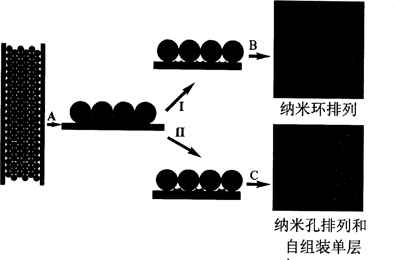
[0034] 2. Put one end of the double substrate with three-dimensional ordered colloidal crystals composed of monodispersed polymer microspheres vertically into the 10 mg / ml aqueous solution of polyvinyl alcohol. Due to capillary action, the aqueous solution of polyvinyl alcohol is filled Fill the space between the two substrates and the voids in the three-dimensional colloidal crystal. After taking it out, it is naturally dried and ultrasonicated for 1 minute in a mixture of methanol and water. A two-dimensional ordered polyvinyl alcohol nanoring arrangement can be obtained on the surface of the substrate (the inner diameter of the ring is about 90 nm, the outer diameter is about 170 nm, and the ring height ...
Embodiment 3
[0036] 1. The preparation of monodisperse polymer microspheres and silicon wafer processing, and the preparation of three-dimensional ordered colloidal crystals composed of monodisperse crosslinked polymer microspheres between two substrates are as described in Example 1.
[0037] 2. Three-dimensional ordered colloidal crystals composed of polymer microspheres with a diameter of 190 nanometers. Place one end of a double substrate with a three-dimensional ordered colloidal crystal composed of monodispersed polymer microspheres into 20% (volume) vertically. Compared with the ethanol solution of butyl titanate, due to capillary action, the ethanol solution of butyl titanate fills the space between the double substrates and the voids in the three-dimensional colloidal crystals. After taking it out, it will be dried naturally, and the colloidal crystal template will be removed after firing at 550℃ for 6 hours, and sonicated in toluene and chloroform for 10 minutes respectively to obtai...
PUM
| Property | Measurement | Unit |
|---|---|---|
| size | aaaaa | aaaaa |
| size | aaaaa | aaaaa |
| thickness | aaaaa | aaaaa |
Abstract
Description
Claims
Application Information