

Vapor growth method for metal oxide dielectric film and PZT film
A technology of vapor phase growth and dielectric film, which is applied in the direction of electrical components, metal material coating technology, circuits, etc., and can solve problems such as continuous alignment difficulties
- Summary
- Abstract
- Description
- Claims
- Application Information
AI Technical Summary
Problems solved by technology
Method used
Image

Examples
example
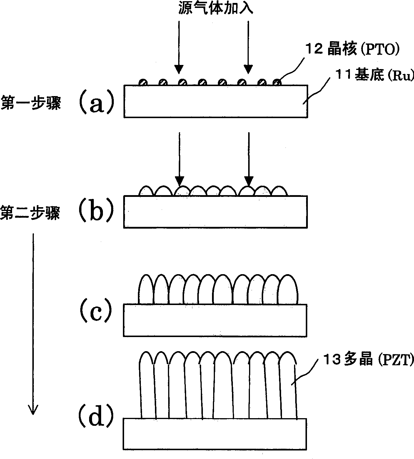
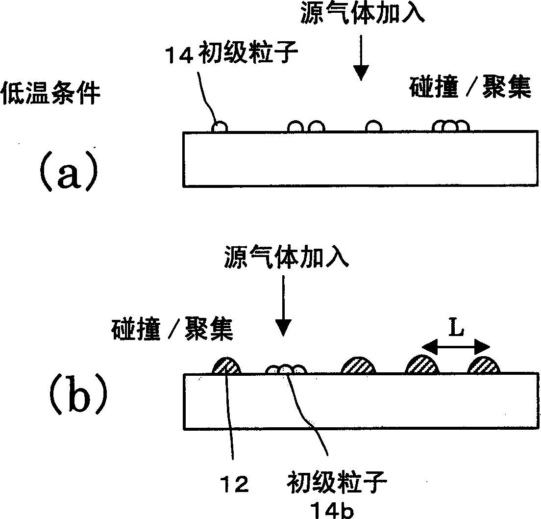
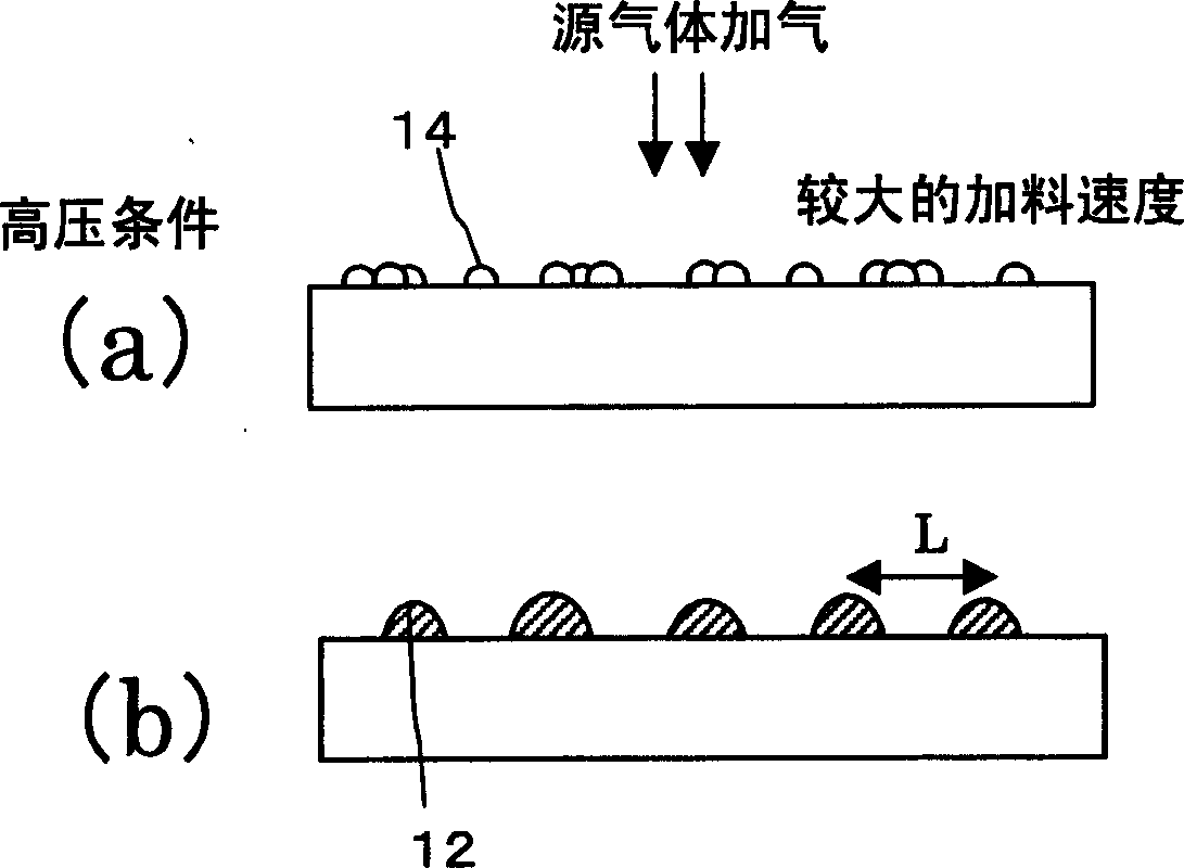
[0106] Examples include: (i) a method wherein all organometallic material gases are used as the material of the metal oxide dielectric under the first deposition condition to form a layer having a perovskite crystal on the surface of the upper base conductive material an initial nucleus of a crystal of the perovskite crystal structure, and then under a second deposition condition, a further film of the perovskite crystal structure is grown on top of the initial nucleus, and (ii) a method wherein only part of the perovskite crystal structure is used under the first deposition condition An organometallic material gas that will be the material of the metal oxide dielectric to form an initial nucleus of a perovskite crystal on the base conductive material, and further grow on top of the initial nucleus under a second deposition condition with calcium A film of titanite crystal structure.
[0107] For the deposition of PZT, in the above method (i), deposition is performed using sou...
Embodiment 1-1
[0145] refer to Figure 28 , Example 1-1 of device production will be described, in which a memory element is produced using a vapor phase growth method according to the present invention. Oxide films are deposited on silicon substrates by wet oxidation. After ions are implanted with dopants such as boron and phosphorus, an n-type or p-type well is formed. Then, gates and diffusion layers are formed as described below. First, a gate oxide film 1601 is formed by wet oxidation, and a polysilicon film 1602 to be a gate is deposited and etched away. A silicon oxide film is deposited on the polysilicon film, and then the silicon oxide film is etched away to form oxide films 1603 of side walls. Next, dopant such as boron or arsenic is ion-implanted to form n-type or p-type diffusion layer 1604 . A Ti film is deposited on the surface, and said Ti film reacts with silicon. Unreacted Ti is etched away to form a Ti silicide layer 1605 on the gate 1602 and the diffusion layer 1604 ....
Embodiment 1-2
[0151] Although in Figure 28 shows the method of separating the capacitors by dry etching after the electrode below the capacitor is formed, a single capacitor can also be prepared by the following method: as shown in Device Production Example 1-2 as a modified method, after separating the capacitor After the lower electrode is Ru / Ti / TiN / Ti, PZT is deposited to form the upper electrode on Ru, and then the upper electrode is separated. refer to Figure 29 Device Production Examples 1-2 are briefly described. exist Figures 29 to 32 in, with Figure 28 The common parts are represented by the same symbols.
[0152] First, as in Production Example 1-1 ( Figure 29 As described in (A)), a transistor is formed on a silicon substrate, and a first interlayer insulating film 1607 and a plug 1608 buried therein are formed. Then, a Ti film 1709, a TiN film 1710, and Ti, which are electrode layers under the capacitor, are deposited sequentially by sputtering, followed by a Ru film ...
PUM
| Property | Measurement | Unit |
|---|---|---|
| Thickness | aaaaa | aaaaa |
| Thickness | aaaaa | aaaaa |
| Leakage current | aaaaa | aaaaa |
Abstract
Description
Claims
Application Information