Micro processing process for silicon nitride ceramic parts
A technology of silicon nitride ceramics and a processing method, applied in the field of ceramic parts processing, can solve the problems of difficulty, high hardness of silicon nitride, and high sintering temperature, and achieve the effect of increasing density
- Summary
- Abstract
- Description
- Claims
- Application Information
AI Technical Summary
Problems solved by technology
Method used
Image
Examples
Embodiment 1
[0027] Using commercially available Si (below 200 mesh, purity 99.99%) powder as a raw material, using silicon nitride balls and a tank lined with silicon nitride, it was ball milled in pure ethanol for 48 hours to obtain a powder with an average diameter of about 5 μm. The Si powder after ball milling is vacuum-dried, filled into a graphite mold, and pre-sintered at about 1250°C using a plasma discharge sintering machine (SPS). The heating rate of SPS is controlled at 100°C / min, and the temperature is lowered after being kept at about 1250°C for 3 minutes. The SPS flake samples were 30 mm in diameter and approximately 5 mm thick. The relative density of the sample after pre-sintering is 80.6%.
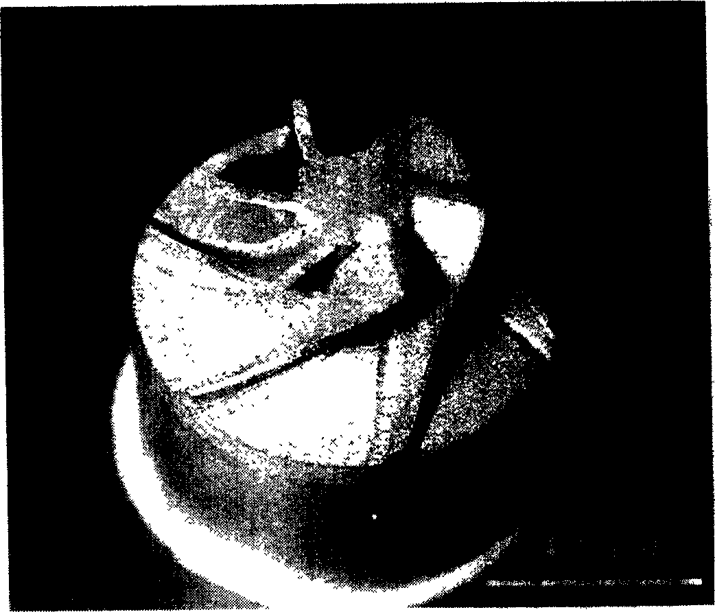
[0028] The SPS pre-sintered body was precisely machined into a micro rotor using a high-speed micro milling machine (F-MACH 442, manufactured by Toshiba Machine). The milling machine used here can achieve 5-axis control, the spindle speed is as high as 60000rpm, and the rotation dev...
Embodiment 2
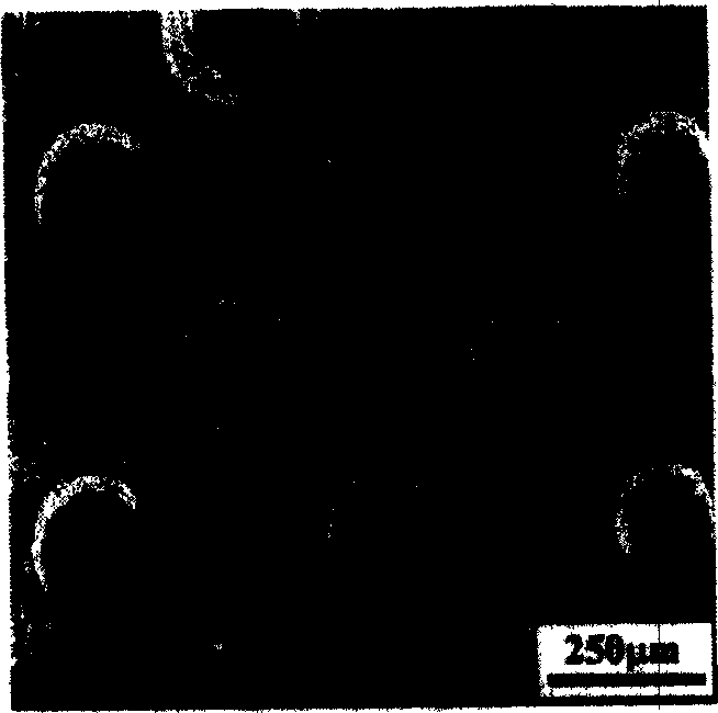
[0031] The calcined temperature was 1100°C, and other conditions were the same as in Example 1 to prepare a silicon calcined body. The relative density of the silicon powder after calcining was 70%, and a micro-hole array was processed on the sheet using a micro electric discharge machining device. Micro-EDM uses tungsten wire as the processing electrode to perform EDM on silicon pre-fired thin slices in air. For a thin sheet with a thickness of about 1.5 mm, a hole can be punched in less than about 1 minute. Figure 3 shows the scanning electron micrographs of the processed micropores. It can be seen that the shape of the micropores is relatively regular, and the inner surface is relatively smooth. The workpiece is placed in a silicon nitride crucible lined with BN powder, and the nitriding reaction is carried out simultaneously with other silicon powders in an industrial nitriding furnace. It was kept at a nitriding temperature of 1360° C. for 1 day. Figure 4 Shown is a s...
Embodiment 3
[0033] The calcining temperature is 1300° C., other conditions are the same as in Example 1, and the relative density of the silicon powder after calcining is 85%. And use a high-speed micro-milling machine (F-MACH 442, manufactured by Toshiba Machinery) to process a micro-rotor (flat plate, equivalent to 2.5 dimensions) smaller than that of Example 1. The micro-rotor is placed in a silicon nitride crucible lined with BN powder, and the nitriding treatment is carried out in the temperature range of 1330-1450 °C. Figure 5 Shown is a scanning electron micrograph of the rotor after nitriding reaction. The diameter of the sample is 5mm, the thickness is 1.2mm, and the thinnest part of the blade is only 70μm. Dimensional measurements before and after reaction sintering showed less than 1% shrinkage in the radial and thickness directions. Such as Figure 6 As shown, X-ray diffraction analysis shows that after reaction sintering, the main component of the micro-rotor is α-Si 3 N ...
PUM
| Property | Measurement | Unit |
|---|---|---|
| particle size | aaaaa | aaaaa |
| diameter | aaaaa | aaaaa |
| thickness | aaaaa | aaaaa |
Abstract
Description
Claims
Application Information


