

Method for preparing one-dimensional nanostructure in anode alumina template
A technology of anodized aluminum and anodic oxidation, which is applied in nanostructure manufacturing, anodic oxidation, chemical instruments and methods, etc., can solve problems affecting the performance test and application of silicon nanowires, wide product diameter distribution, high deposition temperature, etc., and achieve raw material Inexpensive, short time, low synthesis temperature effect
- Summary
- Abstract
- Description
- Claims
- Application Information
AI Technical Summary
Problems solved by technology
Method used
Image

Examples
Embodiment 1
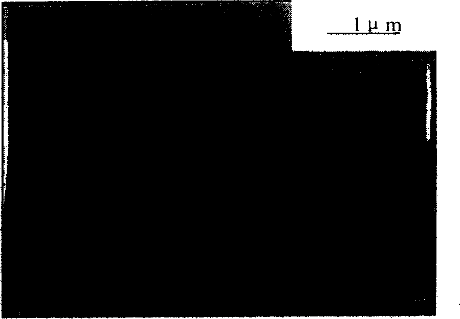
[0017] Degrease the 99.999% high-purity aluminum sheet and anneal it at 500°C for 5 hours, and then polish it in a mixed solution of sulfuric acid and phosphoric acid. After polishing, the aluminum sheet is used as the anode, and the graphite is used as the cathode. The first step of anodizing, after anodizing at 30V for 4h, in 1.8wt%H 2 CrO 4 +6wt%H 3 PO 4 The oxide layer was removed by corrosion in the mixed solution for 2 hours, followed by two-step anodic oxidation with the same parameters as the first step to form the pore structure of porous alumina, and finally with saturated CuSO 4 The solution was used to remove unoxidized aluminum, and the pores were expanded in 5% phosphoric acid for 30 minutes to obtain a porous alumina template with a pore diameter of 30 nm.
[0018] Put the 30nm aperture porous alumina template into the plasma-enhanced chemical vapor deposition reaction chamber, and when the temperature rises to 250°C, 20 sccm of SiH 4 / H 2 Mixed gas (SiH 4...
Embodiment 2
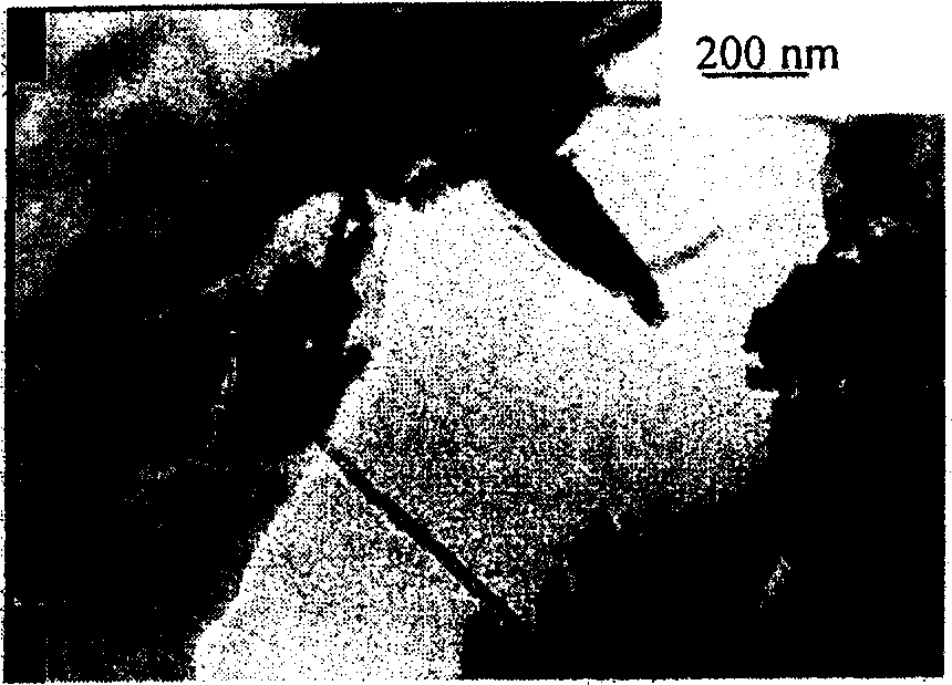
[0020] Degrease the 99.999% high-purity aluminum sheet and anneal it at 500°C for 5 hours, and then polish it in a mixed solution of sulfuric acid and phosphoric acid. After polishing, the aluminum sheet is used as the anode, and the graphite is used as the cathode. The first step of anodizing, after anodizing at 50V for 4 hours, corroded in a mixed solution of phosphoric acid and cadmium acid for 2 hours to remove the oxide layer, and then using the same parameters as the first step for two-step anodizing to form a porous aluminum oxide pore structure , and finally with saturated CuSO 4 Unoxidized aluminum was removed from the solution, and the pores were expanded in 5% phosphoric acid for 60 minutes to obtain a porous alumina template with a pore diameter of 100 nm.
[0021] Put the 100m aperture porous alumina template into the plasma-enhanced chemical vapor deposition reaction chamber, raise the temperature to 400°C, and feed 80sccm of SiH 4 / H 2 Mixed gas (SiH 4 with H...
Embodiment 3
[0023] Degrease the 99.999% high-purity aluminum sheet and anneal it at 500°C for 5 hours, and then polish it in a mixed solution of sulfuric acid and phosphoric acid. After polishing, the aluminum sheet is used as the anode, and the graphite is used as the cathode. The first step of anodizing, after anodizing at 40V for 4h, in 1.8wt%H 2 CrO 4 +6wt%H 3 PO 4 The oxide layer was removed by corrosion in the mixed solution for 2 hours, followed by two-step anodic oxidation with the same parameters as the first step to form the pore structure of porous alumina, and finally with saturated CuSO 4 Unoxidized aluminum was removed from the solution, and the pores were expanded in 5% phosphoric acid for 45 minutes to obtain a porous alumina template with a pore diameter of 60 nm.
[0024] Put the 60nm aperture porous alumina template into the plasma-enhanced chemical vapor deposition reaction chamber, and when the temperature rises to 300°C, 40 sccm of SiH 4 / H 2 Mixed gas (SiH 4 w...
PUM
| Property | Measurement | Unit |
|---|---|---|
| Aperture | aaaaa | aaaaa |
Abstract
Description
Claims
Application Information