Method for fabricating transistor of aluminum-gallium-nitrogen/gallium nitride with high electron mobility

A technology with high electron mobility and fabrication method, which is applied in the fabrication field of aluminum gallium nitride/gallium nitride high electron mobility transistors, and can solve the problem of less two-dimensional electron gas in the channel and the like

Inactive Publication Date: 2006-02-01
INST OF SEMICONDUCTORS - CHINESE ACAD OF SCI
View PDF0 Cites 20 Cited by
  • Summary
  • Abstract
  • Description
  • Claims
  • Application Information

AI Technical Summary

Problems solved by technology

However, there are very few studies on improving the channel two-dimensiona

Method used


Image

  • Method for fabricating transistor of aluminum-gallium-nitrogen/gallium nitride with high electron mobility
  • Method for fabricating transistor of aluminum-gallium-nitrogen/gallium nitride with high electron mobility
  • Method for fabricating transistor of aluminum-gallium-nitrogen/gallium nitride with high electron mobility

Examples


Embodiment

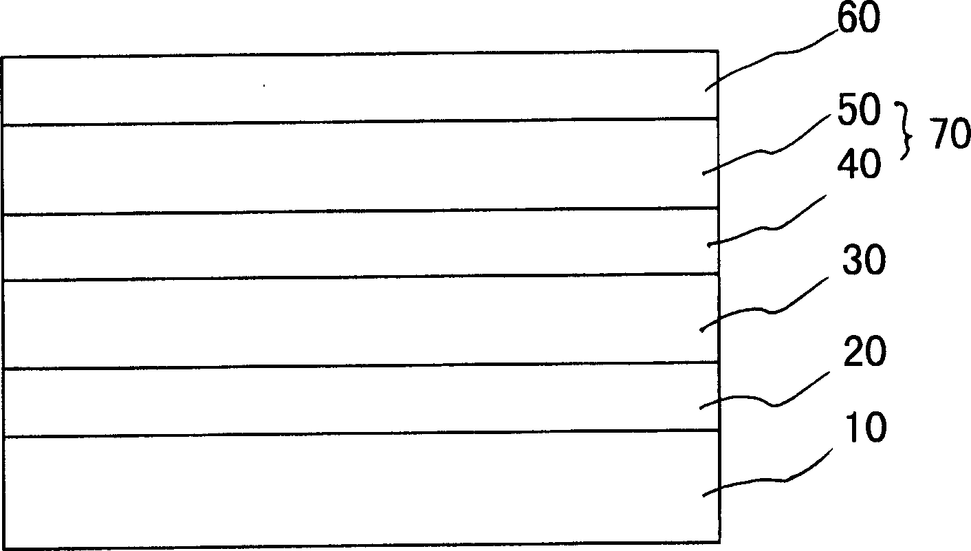
[0027] see again figure 1 Firstly, a layer of aluminum nitride nucleation layer 20 is grown on the substrate sapphire (0001) 10 crystal surface by molecular beam epitaxy technology, the substrate temperature is about 600-700° C., and the growth thickness is about 0.2 nm.

[0028] A thick non-intentionally doped semi-insulating GaN buffer layer 30 was grown on the AlN nucleation layer 20 at a substrate temperature of about 800° C., a nitrogen flow rate of 1.2 sccm, an RF power of 400 W, and a growth thickness of 2 μm.

[0029] A barrier layer 70 with high Al content is grown on the gallium nitride buffer layer 30, including an unintentionally doped space isolation layer 40 and an n-type doped carrier supply layer 50, and the growth thicknesses are 3nm and 21nm respectively, Al The content of Si is 43.2%, and the doping concentration of Si in the carrier supply layer is 2×10 -18 cm -3 .

[0030] Finally, a GaN capping layer 60 is grown with a thickness of 1 nm.

[0031] The ...


PUM

PropertyMeasurementUnit
Thicknessaaaaaaaaaa
Thicknessaaaaaaaaaa
Thicknessaaaaaaaaaa

Abstract

The method includes steps: (1) using method of metallorganics chemical vapor deposition or method of molecular beam epitaxy or method of gas phase epitaxy for hydride develops a thin layer of nucleation layer of aluminum nitride on crystal face of sapphire (0001) substrate or silicon carbide (0001) substrate or silicon (111) substrate; (2) developing a thicker buffer layer of semi insulating gallium nitride in high impedance; (3) developing aluminum-gallium-nitrogen barrier layer in high aluminum content including spatial isolation layer without aluminum-gallium-nitrogen doped, carrier supplying layer with aluminum-gallium-nitrogen doped; (4) developing a covering cap in thin layer of gallium nitride.

Description

technical field [0001] The invention belongs to the technical field of semiconductors, in particular to a method for manufacturing an aluminum gallium nitride / gallium nitride high electron mobility transistor with high two-dimensional electron gas concentration. Background technique [0002] The AlGaN / GaN high electron mobility transistor structure formed by III-V gallium nitride (GaN) and its compound semiconductor materials has very important application prospects in the fields of high-temperature, high-frequency, high-power, radiation-resistant microwave devices and circuits. Mainly because the semiconductor material that makes up the AlGaN / GaN heterostructure has a large band gap, high breakdown electric field, good chemical stability and strong radiation resistance, and also because the GaN material has a high electron saturation drift velocity and peak drift velocity, more importantly because a two-dimensional electron gas with high electron concentration and high elec...

Claims


Application Information

Patent Timeline
IPC IPC(8): H01L21/335H01L29/778
Inventor 王晓亮胡国新王军喜王翠梅曾一平李晋闽
Owner INST OF SEMICONDUCTORS - CHINESE ACAD OF SCI
Why Eureka
Try Eureka