Method for forming semiconductor laser and spot-size converter by once epitaxy

A mode-spot converter and laser technology, applied in semiconductor lasers, lasers, laser parts, etc., can solve the problems of poor device fabrication repeatability, difficult interface processing, and deterioration of mode characteristics, and achieve high differential gain, low cost, and low cost. The effect of device cost reduction

Inactive Publication Date: 2006-04-05
INST OF SEMICONDUCTORS - CHINESE ACAD OF SCI
View PDF0 Cites 14 Cited by
  • Summary
  • Abstract
  • Description
  • Claims
  • Application Information

AI Technical Summary

Problems solved by technology

The three mode spot converters have their own advantages and disadvantages: the thickness of the vertical wedge-shaped waveguide changes gradually from the active area to the output end face
[0005] Although there are many reports on monolithic integrated devices of lasers and speckle converters in the world, the following disadvantages generally exist: 1) Both lasers and speckle converters use buried structures, and the number of epitaxy is many (some as high as 6-7 times), The process is complex and the reliability of the device is low
2) The mode spot converter adopts vertical wedge shape, adopts butt-joint SAG (that is, selective docking) epitaxy technology or gradual c

Method used


Image

  • Method for forming semiconductor laser and spot-size converter by once epitaxy
  • Method for forming semiconductor laser and spot-size converter by once epitaxy
  • Method for forming semiconductor laser and spot-size converter by once epitaxy

Examples


Embodiment

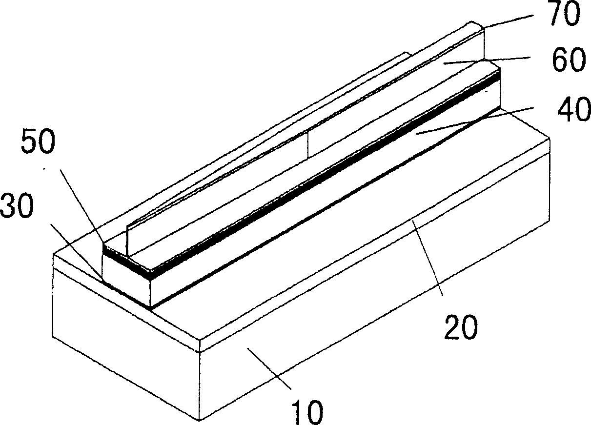
[0062] Please refer to figure 1 , the present invention relates to a kind of preparation method of novel LD-SSC, comprises following preparation steps:

[0063] (1) The 2-inch n-InP substrate undergoes strict decontamination (heating and boiling with ethanol, trichlorethylene, acetone, and ethanol in sequence) → pickling (soaking in concentrated sulfuric acid for 1 to 2 minutes) → water washing (rinsing with deionized water More than 50 times) → after drying treatment, put it into the growth chamber, the growth temperature is 655°C, the growth pressure is 22mbar, and the graphite boat speed is 75-80 rpm.

[0064] (2) On the n-type indium phosphide substrate (100) epitaxially grow n-type indium phosphide buffer layer (0.5 μm thick), lower waveguide layer (thickness 50nm, bandgap wavelength is 1.1 or 1.2 μm), 2.4 μm Indium phosphide space layer, lower optical confinement layer (thickness 80nm, bandgap wavelength 1.1 or 1.2μm), compressive strain quantum well active region, uppe...


PUM

PropertyMeasurementUnit
Thicknessaaaaaaaaaa
Bandgap wavelengthaaaaaaaaaa
Thicknessaaaaaaaaaa

Abstract

Disclosed a method for one time extension forming the semiconductor laser and mode spot switch comprises following steps: (1), on the N type indium phosphide substrate, extending growing the N type indium phosphide breaker, a lower waveguide layer, a 2.4 ª–m indium phosphide space layer, a lower light-limited layer of active region, a compression strain quanta active region, a upper light-limited layer, a P type indium phosphide envelope, and a high doping P type indium gallium arsenide ohmic electrode contract layer; (2), utilizing the wet corrosion process to etch the upper carinate shape of laser and mode spot switch; (3) utilizing the auto-alignment process to etch the lower carinate shape; (4), growing the SiO2 insulating layer and opening a electrode window; (5) decreasing the substrate of extended plate to 100 ª–m, and manufacturing P/N electrodes to be scribed into the tube core of 250í‡600ª–m.

Description

technical field [0001] The invention relates to a method for manufacturing a semiconductor laser and a mode spot converter by means of one epitaxy by one-time LP-MOVPE by using common wet etching and photolithography technology. Background technique [0002] Most modules in optical fiber communication systems are composed of III-V compound semiconductor devices. Each semiconductor device must be connected to at least one optical fiber, so the coupling efficiency between the semiconductor optoelectronic device and the optical fiber is very important. For ordinary glass optical fibers, the refractive index difference between the core layer and the cover layer is very small, generally 5×10 -3 the following. Such a waveguide structure belongs to a weak guiding waveguide, and the distribution of its intrinsic light field is quite diffuse, that is, the intrinsic light spot is relatively large, with a diameter of about 8-10 μm. In III-V compound semiconductors, if the refractive...

Claims


Application Information

Patent Timeline
IPC IPC(8): H01S5/00
Inventor 侯廉平王圩朱洪亮
Owner INST OF SEMICONDUCTORS - CHINESE ACAD OF SCI
Why Eureka
Try Eureka