Nuclear radiation detector and producing technology thereof

A nuclear radiation detector and manufacturing process technology, applied in the field of nuclear radiation detectors, can solve problems such as inability to realize simultaneous measurement, poor long-term stability, poor energy resolution, etc., and achieve excellent electrical characteristics and detection characteristics, and excellent energy resolution The effect of high rate and good position resolution

Inactive Publication Date: 2006-05-17
INST OF MODERN PHYSICS CHINESE ACADEMY OF SCI
View PDF0 Cites 7 Cited by
  • Summary
  • Abstract
  • Description
  • Claims
  • Application Information

AI Technical Summary

Problems solved by technology

For example, the Au-Si surface barrier detector has a large surface leakage current, and its reverse leakage current is mainly determined by the surface leakage current. Therefore, its reverse leakage current is also large, so the noise is large, the energy resolution is poor, and the long-term stabilit

Method used


Image

  • Nuclear radiation detector and producing technology thereof

Examples


Embodiment 1

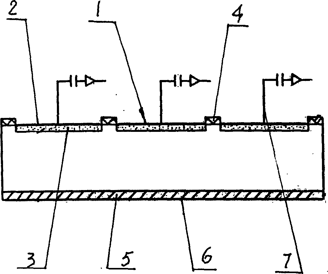
[0032] Example 1: See figure 1 , Nuclear radiation detector, the effective area is 50×20mm 2 Silicon substrate, N type, detection window 1 is composed of 16 parallel detection windows 1, each silicon strip is 3mm wide and 20mm long, with B + The doped area 3 forms a PN junction, on which there is an Al layer 2 and a lead 7; SiO is arranged between the two detection windows 1 2 Insulation partition 4, SiO 2 The width of the partition is 140μm; there is P on the back of the silicon substrate - Doped region 5, forming N + The ohmic contact is covered with an Al layer 6 to form a back electrode. The resistivity of the silicon substrate is 8000-12000Ω·cm, the thickness is 300μm, the crystal orientation is [111], the life of the charged carrier is 1 to 3ms, and there is no dislocation. Lead 7 is connected to the radio frequency cable socket.

Embodiment 2

[0033] Embodiment 2: Manufacturing process of nuclear radiation detector:

[0034] A. Surface oxidation passivation: N-type silicon wafers are used. After cleaning, a 7000 oxide layer is generated at 1030°C. When the surface is oxidized and passivated, the atmosphere of chloride ions is brought in by nitrogen through trichloroethylene liquid. , The flow rate is 0.2 liters / minute, the oxygen flow rate is 6 liters / minute, and the temperature is 950℃~1050℃.

[0035] B. Lithography detector detection window 1.

[0036] C. Ion implantation: implant B on the side of the detector detection window 1 + Ions, the implanted ion concentration is 5×10 13 / cm 2 -1×10 14 / cm 2 .

[0037] D. Remove the SiO on the back of the silicon substrate 2 Layer, inject P - Phosphorus ion concentration is 5×10 15 / cm 2 -1×10 16 / cm 2 . P - Doped region 5 forms N + The thickness of the layer is 1.5 to 2.0 μm.

[0038] E. After ion implantation, annealing to form PN junction and N + For ohmic contact, the annea...


PUM

PropertyMeasurementUnit
Resistivityaaaaaaaaaa
Thicknessaaaaaaaaaa
Widthaaaaaaaaaa

Abstract

The present invention mainly relates to a nuclear radiation detector, in particular, it relates to a position sensitive detector used in the high-energy physics and nuclear physics and its production process. Said detector includes silicon substrate, N-type, it is mainly characterized by that it also includes detection window, it is formed from mutually-parallelized detection windows, it has B+ doped region, forming PN Gunction, on it an Al-layer is set, and is equipped with a lead; between two windows an insulated separating zone is set; back surface of silicon substrate has P- doped region, forming N+ ohmic contact, on it an Al-layer is coated to form back electrode. Said invention also provides the concrete steps of its production method.

Description

Technical field: [0001] The present invention mainly relates to a nuclear radiation detector, in particular to a position sensitive detector used in high-energy physics and nuclear physics and its manufacturing process. Background technique: [0002] Detectors are very important for both high energy physics and nuclear physics. In a nuclear reaction, in order to obtain nuclear-nuclear collision process and its dynamics information, it is necessary to know the angular distribution of the emitted particles or the angular correlation of the emitted particles. For this reason, the measurement of the energy and position (angular distribution) of nuclear reaction products is the most important. For example, in nuclear reactions, the angular distribution of elastic scattering directly reflects the magnitude of nuclear potential and the contribution of angular momentum. The above-mentioned measurement must be done with the help of a position sensitive detector. Over the past few decades,...

Claims


Application Information

Patent Timeline
IPC IPC(8): G01T1/29G01T1/24
Inventor 谭继廉靳根明田大宇宁宝俊王小兵王宏伟段利敏袁小华李松林卢子伟马连荣徐瑚珊
Owner INST OF MODERN PHYSICS CHINESE ACADEMY OF SCI
Why Eureka
Try Eureka