Method for affirming fatal fault in deep-sub-micrometer semiconductor device

A fatal defect, semiconductor technology, applied in the direction of single semiconductor device testing, semiconductor/solid-state device testing/measurement, test sample preparation, etc., can solve problems such as over-corrosion, difficult control, fast corrosion speed, etc., and achieve good repeatability , Ease of use

Inactive Publication Date: 2006-07-12
SEMICON MFG INT (SHANGHAI) CORP +1
View PDF0 Cites 24 Cited by
  • Summary
  • Abstract
  • Description
  • Claims
  • Application Information

AI Technical Summary

Problems solved by technology

However, when this etching solution is used to etch the heavily doped layer in deep submicron ultra-large-scale semiconductor integrated circuits (ULSI), it is prone to severe over-etching and cannot truly reflect the depth of the PN junction. The position of the defect cannot be accurately located
When the etching time is reduced to about 1 second, the etching speed is too fast, the control is difficult, the repeatability of the etching process is poor, and the reliability is poor

Method used


Image

  • Method for affirming fatal fault in deep-sub-micrometer semiconductor device
  • Method for affirming fatal fault in deep-sub-micrometer semiconductor device
  • Method for affirming fatal fault in deep-sub-micrometer semiconductor device

Examples


Embodiment 1

[0031] A method for confirming fatal defects in deep submicron semiconductor devices, comprising the following steps:

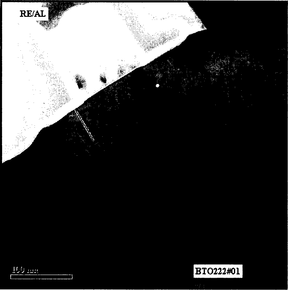
[0032] Step S101, prepare a transmission electron microscope (TEM) test sample with a focused ion beam (FIB) at the position confirmed by MOSAID / PVC, use a transmission electron microscope (TEM) to qualitatively locate and detect the semiconductor device sample, and determine whether there is Silicon crystal defect / dislocation defect, and determine the type of defect.

[0033] Step S102, if there is a defect in the semiconductor device, the sample is detected by the scanning electron microscope (SEM) of the present invention. The corrosion treatment solution corrodes the detection sample. Since the corrosion rates of each film layer in the semiconductor device are different, the corroded sample can be clearly Shows the structure of each film layer;

[0034] In step S103, the section of the sample is inspected by a scanning electron microscope (SEM), so as to...

Embodiment 2

[0037] Scanning electron microscope (SEM) detection sample corrosion treatment solution of another technical scheme of the present invention is, 65% nitric acid (HNO 3 )+acetic acid (CH 3 COOH)+49% hydrofluoric acid (HF)+copper nitrate (Cu(NO 3 ) 2 ) stirring and mixing the mixed acid solution formed.

[0038] The mixing ratio of each component in the mixed acid solution of the present invention is: 20ml 65% HNO 3 : 100mlCH 3 COOH: 1ml 49% HF: (0.8-1.2)gCu(NO 3 ) 2 .

[0039] In the mixed acid solution of the present invention, HNO 3 used as an oxidizing agent, CH 3 COOH was used as a buffer, HF was used as a complexing agent, Cu(NO 3 ) 2 Possesses electrochemical translocation function for improving HNO 3 +CH 3 A mixed acid solution of COOH+HF. The etching time of the mixed acid solution of the invention is appropriate, has an appropriate etching rate, and can ensure better repeatability.

Embodiment 3

[0041] The method for preparing sample by scanning electron microscope (SEM) detection sample corrosion treatment solution of the present invention may further comprise the steps:

[0042] Step 1, 20ml65% nitric acid (HNO 3 )+100ml acetic acid (CH 3 COOH)+1ml49% hydrofluoric acid (HF)+(0.8-1.2 grams) copper nitrate (Cu(NO 3 ) 2 ) stirring and mixing the mixed acid solution formed;

[0043] Step 2, cutting out the sample to be tested from the wafer, showing the profile of the specific position of the sample to be tested;

[0044] In step 3, the sample is soaked in the mixed acid solution prepared in step 1 for corrosion treatment. The time for soaking and corrosion treatment is about 5 seconds, and the corrosion time of the sample can be adjusted according to the sample preparation method used;

[0045] Step 4, the sample after corrosion treatment was rinsed with deionized water, and then dried.

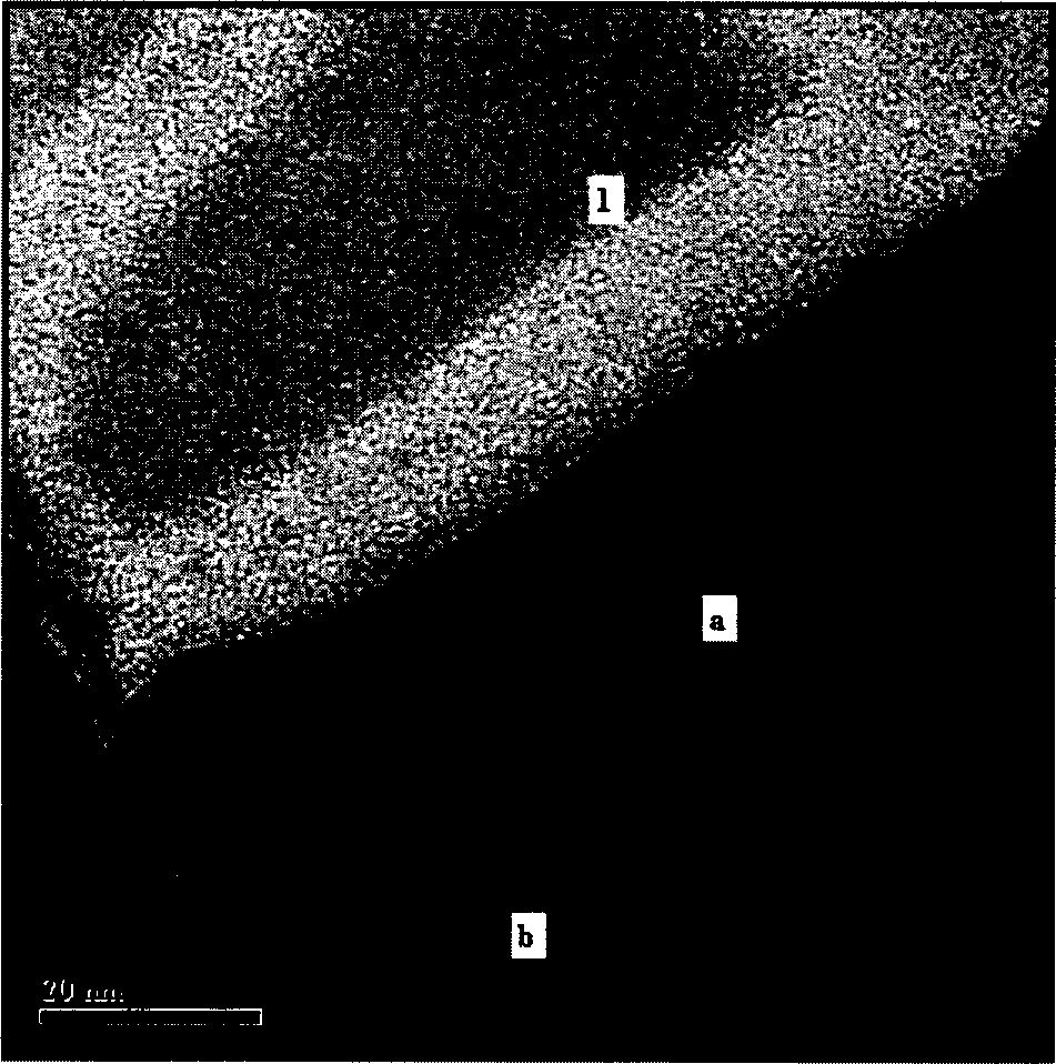
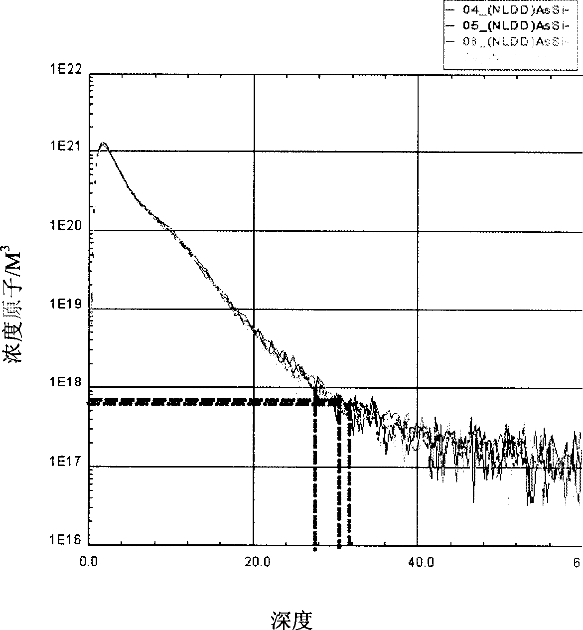
[0046] The contour of the lightly doped drain (NDD) region and the contour o...


PUM


Abstract

The confirmation method for critical defect in semiconductor device of deep sub-micron comprises: step S101, using TEM to qualitative and local detect device sample to determine whether there is silicon crystal defect/dislocation defect and defect type; step S102, if there is defect, using SEM to detect sample, eroding with solution the sample; step S103, detecting sample section with SEM to confirm the film layer position of defect and whether it is fetal. Wherein, the SEM detecting sample erosion solution comprises HNO3, CH3COOH, HF and Cu(NO3)2.

Description

technical field [0001] The invention generally relates to a method for confirming fatal defects in semiconductor devices, in particular to a method for confirming fatal defects in deep submicron semiconductor devices. Background technique [0002] With the rapid development of the performance and manufacturing technology of semiconductor integrated circuits, and the need to reduce the cost of semiconductor integrated circuits, failure analysis plays an extremely important role in the rapidly developing semiconductor industry. [0003] With the development of Ultra Large Scale Integration (ULSI), lightly doped drain (LDD) / source / drain extension (SDE) technology is used in deep sub-micron process systems such as 0.13 μm. In order to make the source / drain expansion region (SDE) shallower to control the short channel effect. A large mass impurity such as indium (In) is used as doping impurity in a small region in the channel close to the source / drain PN junction to control brea...

Claims


Application Information

Patent Timeline
Patent Type & Authority Applications(China)
IPC IPC(8): H01L21/66G01R31/26G01N1/32G01N23/22
Inventor 郭志蓉潘敏秦天陈险峰
Owner SEMICON MFG INT (SHANGHAI) CORP
Why Eureka
Try Eureka