
Surface treating agent for tin or tin alloy material

A surface treatment agent and surface treatment technology, applied in the field of pin structure, can solve the problems of insufficient heat resistance, low repeatability, increase product cost, etc., so as to inhibit the decrease of flux wettability, prevent transformation or oxidation , the effect of excellent oxidation resistance

Inactive Publication Date: 2006-08-23
SONY CORP +2
View PDF3 Cites 24 Cited by
  • Summary
  • Abstract
  • Description
  • Claims
  • Application Information

AI Technical Summary

Problems solved by technology

However, this conventional equipment became unnecessary and had to be abandoned
[0010] (3) Also, if there is any device with insufficient heat resistance, such as electrolytic capacitors, some types of connectors, or thin ICs, its overheating portion is severely affected, and energy (power) consumption increases, thereby increasing product costs
[0020] On the other hand, as disclosed in International Patent Application Publication No. 99-64199, merely adding an organic acid ester or a reducing agent to the flux is not effective in sufficiently suppressing the reactivity of the flux particle surface.
Also, low effective use of solder flux (~80%) due to low repeat printability, resulting in loss and high cost

Method used


Image

  • Surface treating agent for tin or tin alloy material
  • Surface treating agent for tin or tin alloy material
  • Surface treating agent for tin or tin alloy material

Examples


Embodiment 1

[0106] Example 1 shows an example of the reaction of a phosphate ester and a silicon-containing compound.

[0107] 47.3 g (1 mol) of oleyl phosphate (which is a mixture of oleyl acid phosphate with a single OH group and oleyl acid phosphate with two OH groups, manufactured by JOHOKU KAGAKUKOGYO under the trade name JP-518-O, the OH group concentration is 1.5OH group / mole) and 10.4 g (0.5 mol) of tetraethoxysilane (manufactured by KANTOH KAGAKU) were put into a 100 ml eggplant-shaped flask, and heated at 80°C using a magnetic stirrer. Stir at reflux for 1 hour. use 31 P-NMR and 29 The reaction mass was analyzed by Si-NMR. It was found that P-O-Si bonding has been formed, as Figure 7A and 7B shown.

Embodiment 2

[0109] Example 2 shows that the reaction product of a phosphate ester and a silicon-containing compound has improved heat resistance compared to the phosphate ester itself used as a starting material.

[0110] In an Ar atmosphere, T-DTA analysis was performed on the synthesized product (tetraethoxysilane-modified oleyl phosphate) and oleyl phosphate in Example 1 at a heating rate of 20° C. / min. It was found that the decomposition initiation temperature of the former was 278°C and that of the latter was 259°C. This shows that the heat resistance is improved by about 20° C. in terms of the decomposition initiation temperature.

Embodiment 3

[0112] Example 3 shows that the reaction product of a phosphate ester and a silicon-containing compound has improved heat resistance compared to a coating in which the phosphate ester itself was used as a raw material.

[0113] A 10 wt% solution of the synthetic product of Example 1 (tetraethoxysilane-modified oleyl phosphate) and a 10 wt% solution of oleyl phosphate were prepared in isopropanol, respectively. These solutions were respectively applied to sufficiently degreased zinc plated stainless steel plates (zinc plated by SHIN-NITTETSU, non-chromic acid product, 60 mm × 80 mm × 0.6 mm) to form a film on it. Each coating film was about 1 μm.

[0114] Each of these surface-processed zinc-plated stainless steel sheets was left to stand for 30 minutes in a desiccator maintained at a temperature of 150°C. Meanwhile, the temperature of 150° C. is a preheating temperature used in reflow soldering. Before and after heat treatment, FT-IR analysis was performed on the coated fil...


PUM

PropertyMeasurementUnit
thermal resistanceaaaaaaaaaa
diameteraaaaaaaaaa
particle sizeaaaaaaaaaa

Abstract

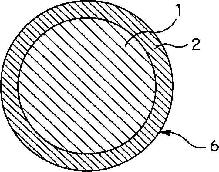
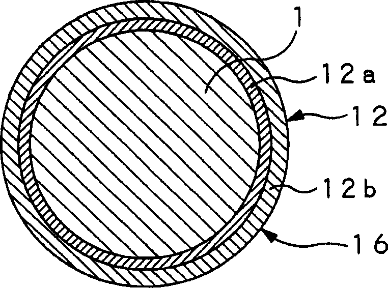
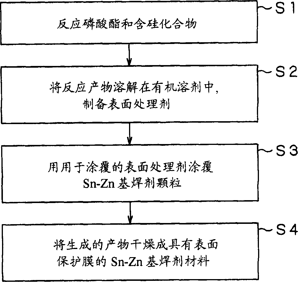
There is disclosed is a method comprising surface-processing a Sn based, Sn alloy based or Sn-Zn alloy based solder particle (1), applied as a coating, such as by electrical plating or melt plating, to the surface of a metal material, such as iron, a steel plate or copper, with a phosphate and a silicium containing compound, to form a protective film (2). There are also disclosed a solder material (6) in which a protective film (2) formed of a phosphate and a silicium containing compound is formed on the surface of the Sn-Zn based solder particle (1), and a solder paste formed of this solder material (6) and the flux.

Description

technical field [0001] The present invention relates to a surface treatment agent for tin or tin alloy materials, tin or tin alloy materials, a method for surface treatment thereof, tin alloy-based flux materials, solder pastes using the same, and tin alloy-based flux materials A manufacturing method, an electronic device, a printed circuit board, and a mount structure related to the electronic device. [0002] The present application contains subject matter related to Japanese Patent Application JP2003-139017 filed in the Japan Patent Office on May 16, 2003, the entire content of which is hereby incorporated by reference. Background technique [0003] Printing in a surface mount device (sometimes referred to as SMD below) or an insert mount device (insert mount device, which is equipped with lead terminals (sometimes referred to as IMD below)) soldering (reflow soldering) to a reflow furnace For board circuits, Sn (tin)-Pb (lead) flux or solder containing such flux particl...

Claims


Application Information

Patent Timeline
Patent Type & Authority Applications(China)
IPC IPC(8): C23C22/03H05K3/34H05K3/28H01L23/12B23K35/22B23K35/26B23K35/363B23K35/02C23C2/08C23C2/26C23C28/00H01L23/498H05K1/18
CPCC23C28/00B23K35/0244C23C2222/20C23C28/021H01L23/49816H01L2924/01004H01L24/48H01L2924/01079H05K2201/10234C23C2/08C23C22/03H01L2224/48247H05K3/3484C23C2/26H01L2924/01019H01L2924/01322H05K2201/0224H01L2924/01078H01L2924/19041H01L2924/01012H05K3/3436H01L2924/01077H01L2224/32245H01L2224/73265H01L2924/181H01L2224/48091H01L2924/14H01L2924/00014Y10T428/12569Y10T428/24917H05K3/3485Y02P70/50H01L2924/00012H01L2924/00H01L2224/45099H01L2224/45015H01L2924/207
Inventor 政时民治鹤崎新熊谷正志大内高志木名濑隆杉冈理贵中野健
Owner SONY CORP
Learn More