Electrode array microchip sensor, preparation method and application therefor

An electrode array and microchip technology, used in instruments, scientific instruments, material analysis by electromagnetic means, etc., can solve the problems of system target measurement accuracy error, detection system interference, increase detection cost, etc., and achieve industrialized batch size. The effect of reducing the cost of detection and production, low detection limit

Inactive Publication Date: 2006-11-22
FUDAN UNIV +1
View PDF3 Cites 20 Cited by
  • Summary
  • Abstract
  • Description
  • Claims
  • Application Information

AI Technical Summary

Problems solved by technology

The existence of the labeling process can easily cause interference to the detection system, causing errors in the measurement accuracy of the system target, and the generated interference signal will also affect the specificity of the measurement; and the existence of the labeling process further increases the detection cost.
[0007] From the above analysis, it can be seen that although the electrochemical immunoprotein chip has broken through the limitation of single channel at this stage, it still needs to be further developed in terms of integration and miniaturization, so that the advantages of electrochemical detection in immunoprotein chips can be fully utilized.

Method used


Image

  • Electrode array microchip sensor, preparation method and application therefor
  • Electrode array microchip sensor, preparation method and application therefor
  • Electrode array microchip sensor, preparation method and application therefor

Examples


Embodiment 1

[0049] Embodiment 1 Fabrication of Electrode Array Microchip Sensor

[0050] 1. Pretreatment of monocrystalline silicon wafers

[0051] (1) Cleaning the surface of a single crystal silicon wafer with a diameter of 2.5-7.5 inches is first cleaned according to the following process. 1# liquid (NH 3 :H 2 o 2 :H 2 O=1:2:7) boiled for 10 minutes, rinsed with deionized water for 15 minutes; then use 2# liquid (HCl: H 2 o 2 :H 2 (0=1:2:7) was boiled for 10 minutes, rinsed with deionized water for 15 minutes, and dried under an infrared lamp.

[0052] (2) Oxidation to generate SiO 2 Insulating substrate: In the domestic oxidation furnace, in the presence of oxygen, a layer of SiO with a thickness of about 500 nanometers is formed by thermal oxidation at 500 °C 2 TLC.

[0053] 2. Electrode fabrication

[0054] (1) The production of the working electrode and the counter electrode uses the German Karl Hughes photolithography machine for the first photolithography (the remainin...

Embodiment 2

[0058] Example 2 High-throughput detection of multiple disease markers in human serum samples

[0059] 1. Fabrication of Multichannel Electrode Array Microchip Sensors

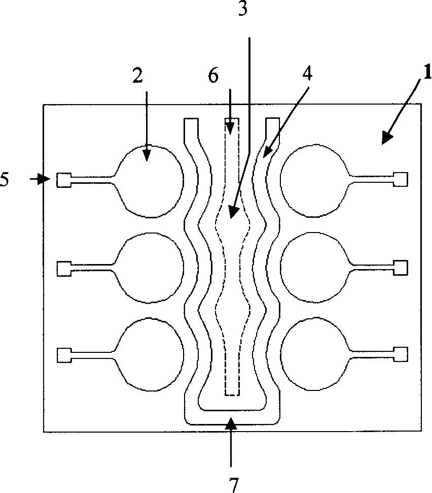
[0060] Referring to the method of Example 1, a 6-channel electrode array microchip sensor was fabricated.

[0061] 2. Generation of Antibody-Polymer Membrane

[0062] Add 50 microliters of 10 millimolar pH 7.0 phosphate buffer solution containing 10 millimolar o-phenylenediamine polymerizable monomer and 3 micrograms / ml antibody to be copolymerized into the electrolytic cell formed on the surface of the microchip sensor . Connect each lead wire of the electrode array microchip sensor to the corresponding working electrode, counter electrode and reference electrode connection port of the multi-channel electrochemical workstation. Antibody-polymer films were generated by cyclic voltammetry (CV) at room temperature. The experimental conditions are as follows: scanning range (0-0.8V), scanning speed (100 mV / s)...


PUM

PropertyMeasurementUnit
diameteraaaaaaaaaa
widthaaaaaaaaaa

Abstract

The related multi-channel array micro-chip sensor integrated tri-electrode system comprises: an electrode array micro-chip with a work electrode array, a counter electrode and a reference electrode; and a detection cell with area less than 50um. This invention improves detection sensitivity, accuracy and speed, reduces cost, and fit to wide application.

Description

technical field [0001] The invention relates to the field of electrode array microchip sensors. Specifically, the present invention designs a multi-channel array microchip sensor integrating a three-electrode system. The invention also provides the preparation method and application of the microchip sensor. Background technique [0002] Miniaturization, integration, intelligence and high throughput have become important research directions in the field of biological / chemical analysis. With their distinct advantages, they have achieved remarkable achievements in the fields of disease diagnosis and prediction, drug screening, gene expression profile analysis, discovery of new genes, gene mutation detection and gene sequencing, including from academic research to commercial applications, etc. The field has been fully developed. The analysis and detection system is miniaturized and integrated on a tiny chip, which can realize many characteristics such as less sample requireme...

Claims


Application Information

Patent Timeline
Patent Type & Authority Applications(China)
IPC IPC(8): G01N27/00G01N33/48
Inventor 孔继烈史绵红余绍宁周佳黄宜平
Owner FUDAN UNIV
Why Eureka
Try Eureka