High-luminance chip of luminescent tube in GaN base, and preparation method

A light-emitting tube and high-brightness technology, which is applied in the field of optoelectronics, can solve problems such as process sensitivity, and achieve the effects of increasing output efficiency, improving thermal characteristics, and improving electrical conductivity

Inactive Publication Date: 2006-12-06
PEKING UNIV
View PDF0 Cites 33 Cited by
  • Summary
  • Abstract
  • Description
  • Claims
  • Application Information

AI Technical Summary

Problems solved by technology

[0005] The nano-compression patterned LED light-emitting surface technology we propose here, the template prepared at one time can be repeatedly used by pressing, and can be directly applied to the LED light-emitting surface of any structure, completely avoiding the introduction of various micro-processing methods to the material. damage, solve the problem that the quality of P-type GaN materials is sensitive to processes such as ion etching heat treatment, and cannot dire

Method used


Image

  • High-luminance chip of luminescent tube in GaN base, and preparation method
  • High-luminance chip of luminescent tube in GaN base, and preparation method
  • High-luminance chip of luminescent tube in GaN base, and preparation method

Examples


Embodiment 1

[0022] The technical scheme of embodiment one:

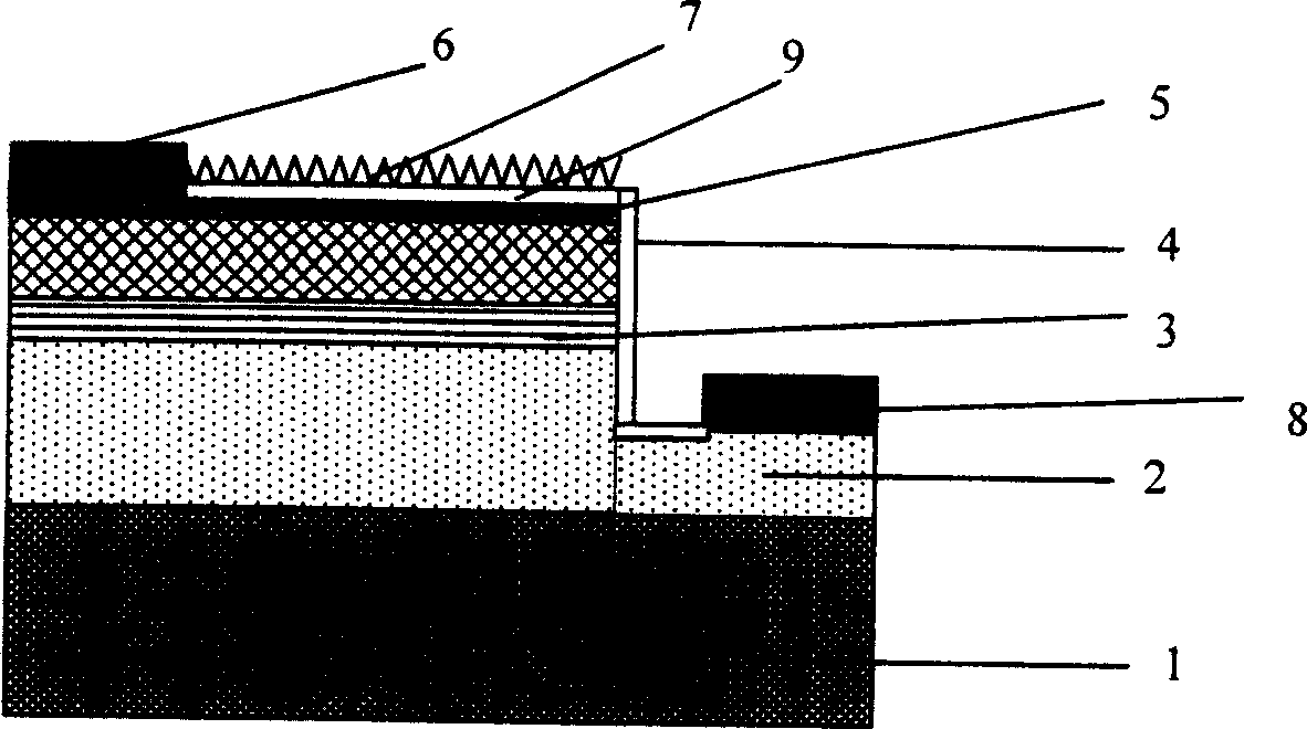
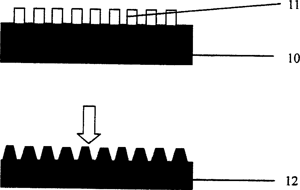
[0023] Figure 2a-2d It is a flow chart of the manufacturing process of the GaN-based light-emitting diode die with a surface microstructure; the manufacturing process and chip structure of Embodiment 1 will be described in detail below with reference to FIG. 2 .

[0024] 1) Prepare an LED chip with a conventional structure, the specific steps are as follows:

[0025] a) A mesa is first etched on the GaN-based LED epitaxial wafer grown on the sapphire substrate 1, and the mesa is etched through the active region 3 to the N-type GaN material 2;

[0026] b) Deposit Ni / Au (5nm / 5nm) P-type ohmic contact layer 5 on the P-type GaN material 4 on the mesa, and after alloying at 500° C. for 2-10 minutes in an oxygen atmosphere, rinse off the surface NiO with oxalic acid aqueous solution.

[0027] c) Prepare an N-type ohmic contact layer 8 on the N-type GaN material 2 under the mesa, which is composed of Ti / Al (5nm / 20-200nm), and then d...

Embodiment 2

[0032] The technical scheme of embodiment two:

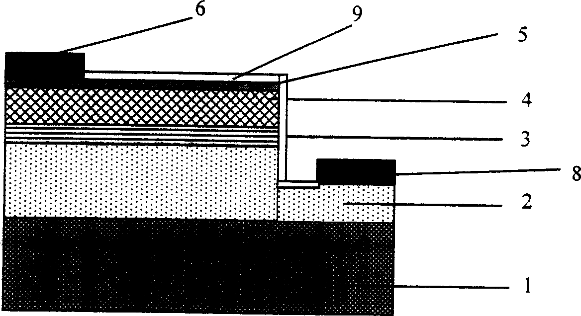
[0033] Figure 3a ~ 3f It is a flow chart of the manufacturing process of the GaN-based light-emitting diode tube core with a surface microstructure; the preparation process and chip structure of the second embodiment will be described below with reference to FIG. 3 .

[0034] 1) Prepare the LED chip with the vertical structure of the upper and lower electrodes, the specific steps are as follows:

[0035] a) On the P-type GaN material 4 on the GaN-based LED epitaxial wafer of the sapphire substrate, the transparent electrode Ni / Au (5nm / 5nm) 5 is evaporated on a large area, and then alloyed at 500° C. for 2-10 minutes under an oxygen atmosphere, and used Aqueous oxalic acid rinses off the surface NiO. Evaporate a multi-layer reflective film 13 on the transparent electrode, consisting of Ni / Ag / Ti / Au (10nm / 200nm / 20nm / 200nm), wherein Ag is a reflective layer, and Au is a metal barrier layer, such as Figure 3a .

[0036] b) On t...


PUM


Abstract

The technical scheme discloses high brightness LED structure with graphic surface and microstructure. Using Nano pressing technique prepares each graphic film from organic material on luminous surface of LED so as to form microstructure on LED surface in favor of transgression of emitting light from active region, for example micrographics with structure or coarsening, and photon crystal structure. Introducing the said micrographics on surface makes interfacial area of light emergence medium increase. The increased surface presents great lot small areas unordered arranged. Emergence of light from active region and interface of medium is at random in a certain extent. The invention improves directions of emergence light, increases probability of emergence so as to raise light extraction efficiency and external quantum efficiency of LED.

Description

technical field [0001] The invention belongs to the field of optoelectronic technology, and in particular relates to the structure of a high-brightness GaN-based light-emitting diode (LED) chip and its preparation technology. Including the use of ultraviolet lasers with a wavelength shorter than the GaN bandgap absorption wavelength to peel off the GaN-based LED epitaxial layer grown on the sapphire substrate, and on this basis combined with nano-pressing technology to form a GaN-based high-brightness light-emitting diode chip structure and its preparation technology Program. Background technique [0002] The internal quantum efficiency and external quantum efficiency of light-emitting diodes determine the total light extraction efficiency and device brightness of LEDs. At present, most GaN-based light-emitting diodes are grown by epitaxy on a sapphire substrate (mismatch up to 15%) that has a large lattice mismatch with GaN materials, which directly causes the material dis...

Claims


Application Information

Patent Timeline
IPC IPC(8): H01L33/00H01L51/50H01S5/00
Inventor 康香宁章蓓陈勇包魁徐科张国义陈志忠胡晓东
Owner PEKING UNIV
Why Eureka
Try Eureka