Y-Ba-Cu-O coating conductor with conducting buffer layer and preparing process

A conductive buffer, yttrium barium copper oxide technology, applied in superconducting/high-conducting conductors, usage of superconducting elements, manufacturing/processing of superconducting devices, etc., can solve problems such as poor superconducting performance of YBCO superconducting film, and achieve experimental results The parameters are easy to control, the oxygen diffusion coefficient is small, and the effect of good thermal expansion coefficient transition characteristics

Inactive Publication Date: 2007-01-31
INST OF PHYSICS - CHINESE ACAD OF SCI
View PDF0 Cites 11 Cited by
  • Summary
  • Abstract
  • Description
  • Claims
  • Application Information

AI Technical Summary

Problems solved by technology

[0003] The superconducting performance of the YBCO superconducting film deposited directly on the metal substrate is very poor, so a buffer layer must be added on the metal substrate

Method used


Image

  • Y-Ba-Cu-O coating conductor with conducting buffer layer and preparing process
  • Y-Ba-Cu-O coating conductor with conducting buffer layer and preparing process
  • Y-Ba-Cu-O coating conductor with conducting buffer layer and preparing process

Examples


Embodiment 1

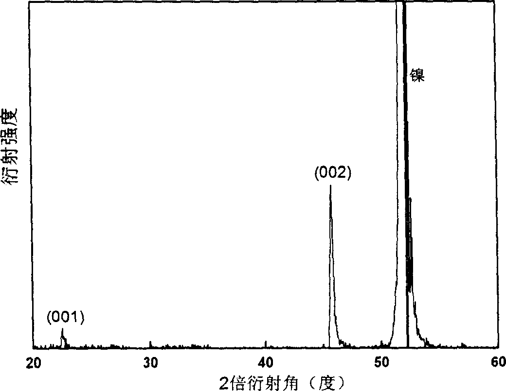
[0032] Embodiment 1: the present embodiment has SrTi 0.95 Nb 0.05 o 3 YBCO-coated conductors for the conductive buffer layer, comprising a cubic textured Ni substrate with a thickness of 0.2 μm, on which a layer of SrTi with a thickness of 100 nm is grown 0.95 Nb 0.05 o 3 conductive buffer layer, then the SrTi 0.95 Nb 0.05 o 3 On the conductive buffer layer, a yttrium barium copper oxide superconducting layer with a thickness of 600nm is grown again.

[0033] The method of this embodiment utilizes the conventional pulsed laser deposition process and is carried out in pulsed laser deposition equipment; the metal baseband is selected from the Ni baseband with cubic texture, and SrTi with 100nm is prepared thereon. 0.95 Nb 0.05 o 3 The yttrium barium copper oxide coated conductor of the conductive buffer layer, its specific process is as follows:

[0034] 1. The SrTi prepared by high temperature sintering 0.95 Nb 0.05 o 3 The ceramic target is installed on the target...

Embodiment 2

[0045] Embodiment 2: the present embodiment has SrTi 0.7 Nb 0.3 o 3 YBCO-coated conductors for conductive buffer layers, including a cubic textured Ni substrate with a thickness of 0.2 μm, and a layer of SrTi with a thickness of 500 nm grown on the cubic textured Ni substrate 0.7 Nb 0.3 o 3 conductive buffer layer, the SrTi 0.7 Nb 0.3 o 3 The conductive buffer layer grows a yttrium barium copper oxide superconducting layer with a thickness of 600nm.

[0046] Fabrication of SrTi with 500nm on cubic textured Ni substrate 0.7 Nb 0.3 o 3 The conductive buffer layer of the YBCO coated conductor is as follows:

[0047] The preparation method of the present embodiment is different from embodiment 1 except step 1 and the process of preparing the conductive buffer layer, all the other repeat the steps in the embodiment 1, the process of preparing the conductive buffer layer is as follows:

[0048] Change to pre-sintered SrTi on the target support 0.7 Nb 0.3 o 3 ceramic ta...

Embodiment 3

[0051] Embodiment 3: the present embodiment has SrTi 0.9 In 0.1 o 3 The yttrium barium copper oxide coated conductor of the conductive buffer layer includes a Ni alloy substrate with a cubic texture of 0.2 μm in thickness, and a layer of SrTi with a thickness of 200 nm is grown on the Ni alloy substrate with a cubic texture. 0.9 In 0.1 o 3 conductive buffer layer, the SrTi 0.9 In 0.1 o 3 On the conductive buffer layer, a yttrium-barium-copper-oxygen superconducting layer with a thickness of 600nm is grown again.

[0052] Fabrication of SrTi with 200nm on Ni alloy substrate with cubic texture 0.9 In 0.1 o 3 The conductive buffer layer of the YBCO coated conductor is as follows:

[0053] 1. The SrTi prepared by high temperature sintering 0.9 In 0.1 o 3 The ceramic target is installed on the target holder in the reaction chamber;

[0054] 2. Remove the oxide impurities on the surface of the Ni alloy substrate;

[0055] 2a) Using acetone, alcohol, and deionized water ...


PUM

PropertyMeasurementUnit
thicknessaaaaaaaaaa
thicknessaaaaaaaaaa
thicknessaaaaaaaaaa

Abstract

The invention relates to yttrium barium copper oxygen coating conductor with conduct buffer layer. It includes adulterated strontium titanate conduct buffer layer and YBCO superconducting layer. The former includes niobium strontium titanate SrTi1-xNbxO3, indium strontium titanate SrTi1-xInxO3, or lanthanum strontium titanate Sr1-xLaxTiO3 which x is between 5mol% and 30mol%. Its manufacturing method includes the following steps: using pulsed laser deposition technique to adjust pressure at 1-5Pa in reaction chamber, substrate temperature at 700-800 degree centigrade, conductive film deposition thickness at 30-50nm; pumping out the mixed gas from the reaction chamber; filling 10-2Pa oxygen with 99.99% purity; keeping the temperature not change; making the deposition thickness of the adulterated strontium titanate conductive film at 100-500nm.

Description

technical field [0001] The present invention relates to yttrium barium copper oxide coated conductor (YBCO) with conductive buffer layer and preparation method thereof, particularly relate to the doped strontium titanate conductive buffer layer of texture prepared on the metal base tape by pulsed laser deposition technology, and then A method for preparing a high-quality YBCO superconducting film using this as a template. Background technique [0002] As the second generation of high-temperature superconducting tape, YBCO coated conductor has the characteristics of high critical current density (Jc), good critical current density-magnetic field (Jc-B) characteristics and low price, and it is likely to replace bismuth-based high-temperature conductors in the future. Superconducting strips are used in the field of superconducting strong electric technology, such as motors, motors, transformers, current limiters, magnets, superconducting energy storage, nuclear magnetic resonan...

Claims


Application Information

Patent Timeline
Patent Type & Authority Applications(China)
IPC IPC(8): H01B1/00H01B5/00H01B12/00H01B12/06H01L39/12H01L39/24
CPCY02E40/64Y02E40/642Y02E40/60
Inventor 王淑芳周岳亮赵嵩卿韩鹏陈正豪吕惠宾金奎娟程波林何萌杨国桢
Owner INST OF PHYSICS - CHINESE ACAD OF SCI
Why Eureka
Try Eureka