Electric field tuning of PbS quantum dots for high efficiency solar cell application
- Summary
- Abstract
- Description
- Claims
- Application Information
AI Technical Summary
Benefits of technology
Problems solved by technology
Method used
Image


Examples
example 1
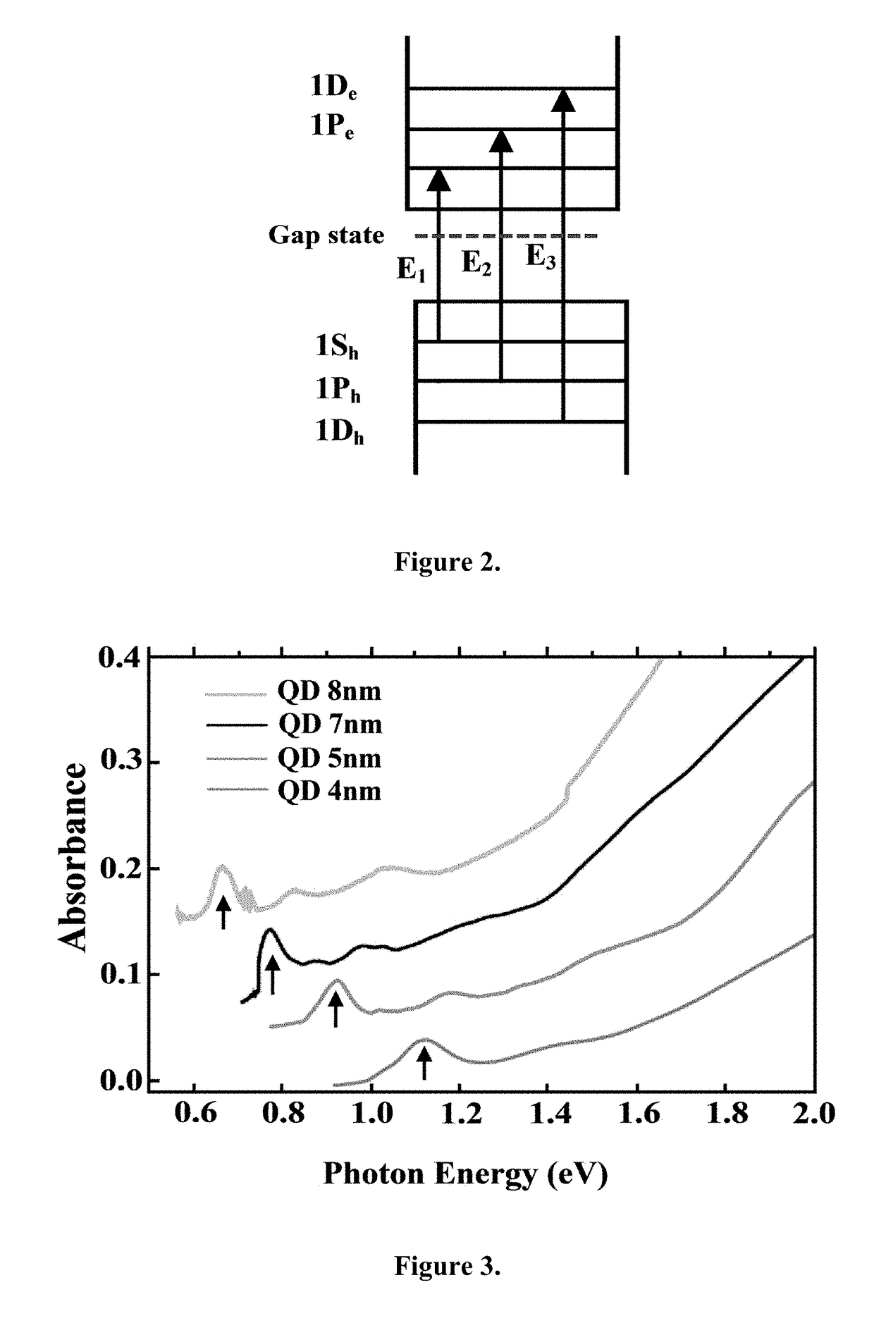
[0053]The quantum dots (e.g. lead selenide (PbSe) and PbS quantum dots) with different-sized capping ligands were synthesized using a modified colloidal synthesis procedure. Briefly, a colloidal solution containing 9-10 nm PbSe nanoparticles was formed by a solvothermal technique, forming QDs coated with oleic acid that prevents agglomeration (Dedigamuwa, et al., Enhanced charge-transport in surfactant-free PbSe quantum dot films grown by a laser-assisted spray process. Appl Phys Lett. 2009, 95(12), 122107). The precipitated PbSe nanocrystals were redispersed in hexane. The surfactants cause the particles to separate by about 2-3 nm. As an example, FIG. 7 shows an absorption spectrum of 9 nm PbSe quantum dots synthesized by a modified colloidal synthesis procedure. The inset shows a high resolution transmission electron micrograph (HRTEM) demonstrating uniform size distribution, which is confirmed by the narrow FWHM of the absorption peak at about 0.65 eV.
[0054]A colloidal synthesis...
example 2
[0056]An indium tin oxide (ITO) with and Corning® low alkaline earth boro-aluminosilicate glass substrate (Delta Technology, Inc.) having a nominal sheet resistance of 4-10 Ω / square was pre-cut 4″×4″, and patterned for use as a substrate. Any patterning known in the art is acceptable. For example, the substrate is patterned using a positive photo resist, Shipley 1813, spin coated at 4500 rpm and soft baked on a hotplate for 3 minutes at 90° C. The structure was then exposed to a UV lamp for 1.4 seconds using a constant intensity mode set to 25 watts. The structure was developed for about 2.5 minutes using Shipley MF319, rinsed with water, and hard-baked at 145° C. for 4 minutes. Any excess photoresist was cleaned off with acetone and cotton. The substrate was etched 5-11 minutes with a solution of 20% HCl and 7% HNO3 at 100° C.
[0057]A layer of quantum dots is then applied to the patterned substrate. A solution of PbS quantum dots was drop-casted or spin coated onto the substrate. Ex...
example 3
[0062]Devices were prepared for TOF and CELIV measurements. While complimentary planar structure (FET device) or sandwich structure (normal PV device) can be fabricated for the analysis, sandwich structure devices were fabricated.
[0063]Devices can be fabricated in an oxygen and humidity controlled device fabrication facility, which includes an customized Mbraun MB200M glove box system, integrated with {acute over (Å)}ngstrm {acute over (Å)}mod four-source co-deposition system for high vacuum (−7 torr) metal and organic deposition, as described in U.S. patent application Ser. No. 12 / 862,260. A built-in Laurel programmable spin-coater allows the fabrication of devices inside the inert gas atmosphere. This setup provides an ideal controlled environment for device stability studies. Flow charts of the fabrication processes for the sandwich PV device and planar FET device, are shown in FIGS. 10 and 11, respectively. The fabrication process for the sandwich PV device is further described ...
PUM
| Property | Measurement | Unit |
|---|---|---|
| Time | aaaaa | aaaaa |
| Electric potential / voltage | aaaaa | aaaaa |
| Electric potential / voltage | aaaaa | aaaaa |
Abstract
Description
Claims
Application Information