Mask blank, method for manufacturing transfer mask, and method for manufacturing semiconductor device

a technology of transfer mask and mask, applied in the field of mask blank, method for manufacturing transfer mask, and method for manufacturing semiconductor device, can solve the problem of directly affecting the dimensional accuracy of fine, and achieve the effect of accurately forming a fine transfer pattern, reducing side etching amount, and reducing lwr

Active Publication Date: 2022-03-22
HOYA CORP
View PDF23 Cites 2 Cited by
  • Summary
  • Abstract
  • Description
  • Claims
  • Application Information

AI Technical Summary

Benefits of technology

[0047]According to the mask blank of this disclosure having the above-mentioned configurations, the mask blank has a structure in which a light shielding film made of a silicon-based material or a tantalum-based material and a hard mask film made of a chromium-based material are laminated on a transparent substrate in this order. With the mask blank, even if the hard mask film is patterned through dry etching in a high-bias condition using, as a mask, a resist film having a pattern to be formed on the light shielding film and using a mixed gas of a chlorine-based gas and an oxygen gas, it is possible to reduce a side etching amount generated on a pattern side wall of the hard mask film and to reduce LWR also. Thus, it is possible to accurately form a fine transfer pattern on the hard mask film. Furthermore, by patterning the light shielding film using, as a mask, the hard mask film provided with the transfer pattern, it is possible to accurately form a fine pattern on the light shielding film also. In addition, by using the mask blank, it is possible to manufacture a transfer mask provided with a high-accuracy fine transfer pattern. Furthermore, by carrying out pattern transfer on a resist film of a semiconductor substrate using the transfer mask, it is possible to manufacture a high-quality semiconductor device provided with a device pattern excellent in pattern accuracy.

Problems solved by technology

Therefore, dimensional accuracy of the pattern formed on the transfer mask directly affects dimensional accuracy of a fine pattern to be prepared using the transfer mask.

Method used


Image

  • Mask blank, method for manufacturing transfer mask, and method for manufacturing semiconductor device
  • Mask blank, method for manufacturing transfer mask, and method for manufacturing semiconductor device
  • Mask blank, method for manufacturing transfer mask, and method for manufacturing semiconductor device

Examples


example 1

[0139]Example 1 relates to a mask blank for use in manufacture of a transfer mask (binary mask) using an ArF excimer laser having a wavelength of 193 nm as exposure light, and to manufacture of the transfer mask.

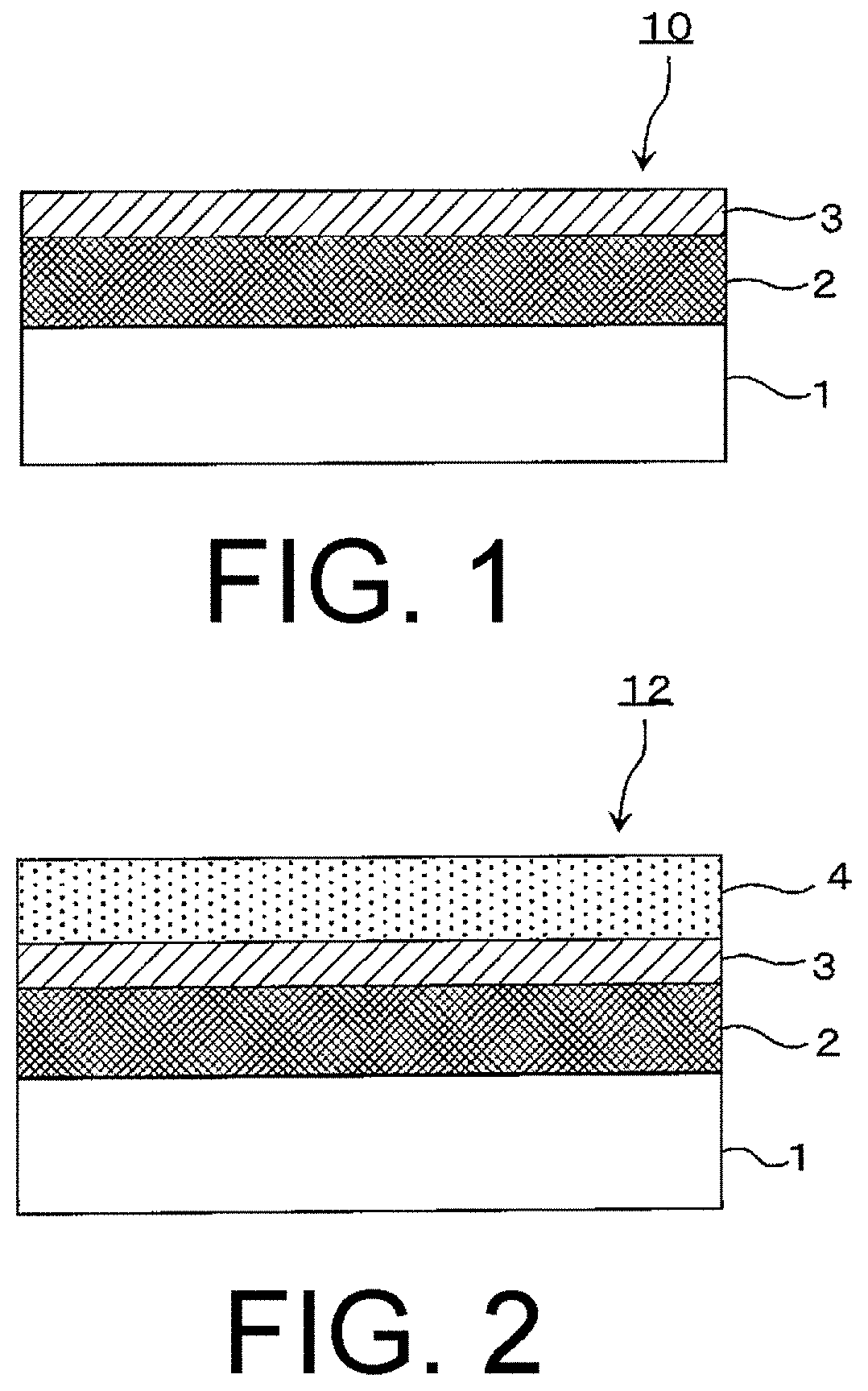
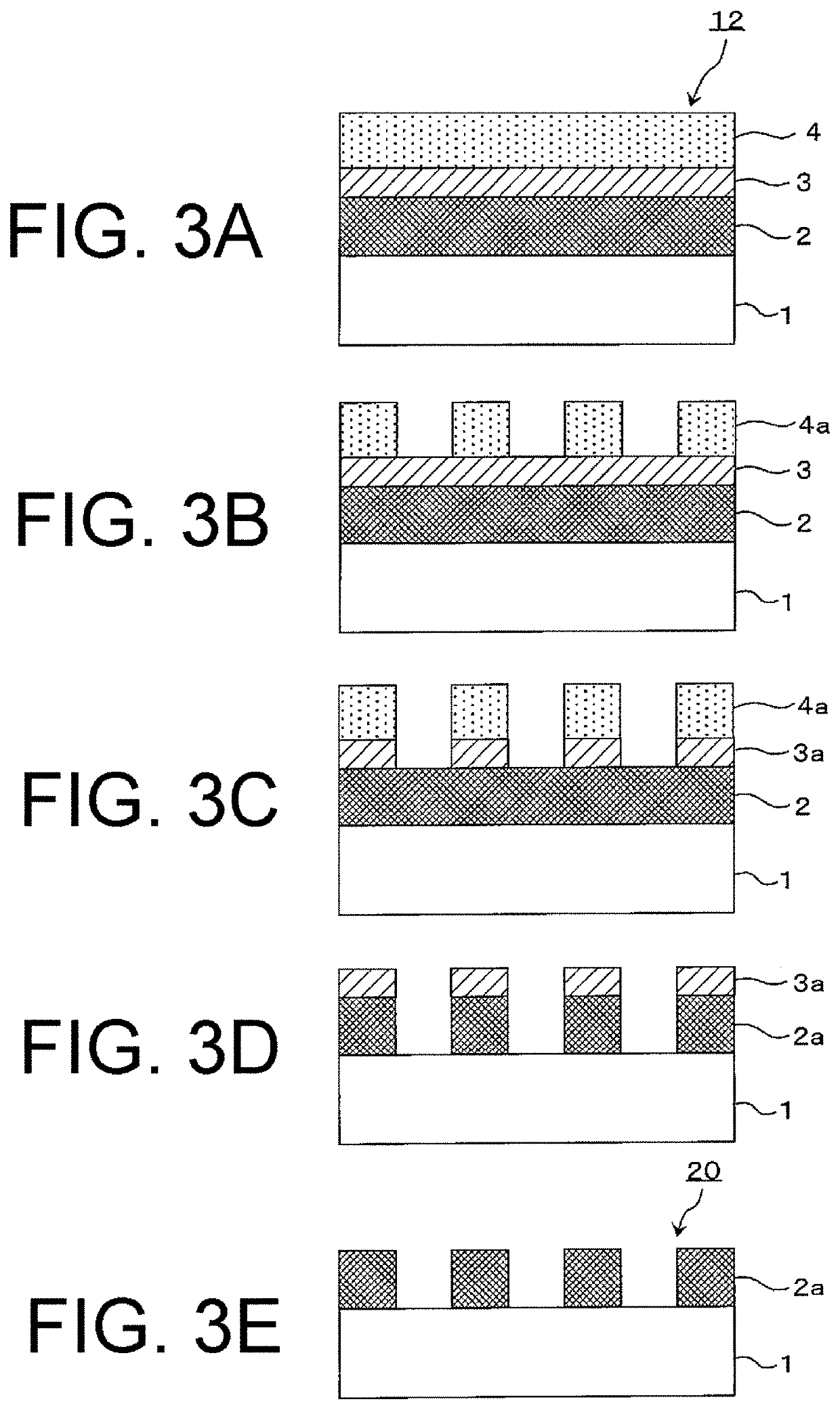
[0140]A mask blank 10 used in Example 1 has a structure in which a light shielding film 2 and a hard mask film 3 are laminated on a transparent substrate 1 in this order, as illustrated in FIG. 1. The mask blank 10 was manufactured as follows.

[0141]The transparent substrate 1 (having a size of about 152 mm×152 mm×thickness of about 6.35 mm) made of synthetic quartz glass was prepared. In the transparent substrate 1, a main surface and an end face are polished to a predetermined surface roughness (for example, the main surface has Rq of 0.2 nm or less).

[0142]Next, the transparent substrate 1 was placed in a single-wafer RF sputtering apparatus. Using a silicon (Si) target and a mixed gas of krypton (Kr), helium (He), and nitrogen (N2) (flow rate ratio Kr:He:N2=10:100:1, press...

example 2

[0171]A mask blank 10 in Example 2 was prepared in the manner similar to Example 1 except a hard mask film 3. The hard mask film 3 in Example 2 was formed in a film forming condition changed from that of the hard mask film 3 in Example 1 as follows.

[0172]Specifically, a synthetic quartz substrate provided with the light shielding film 2 comprising the SiN film in Example 1 was placed in a single-wafer DC sputtering apparatus. Using a target comprising chromium, reactive sputtering was carried out in a mixed gas atmosphere of Argon (Ar), carbon dioxide (CO2), and helium (He) so that the hard mask film 3 comprising a CrOC film containing chromium, oxygen, and carbon was formed on the light shielding film 2 to the thickness of 9 nm.

[0173]In the above-mentioned manner, the mask blank 10 of Example 2 was prepared.

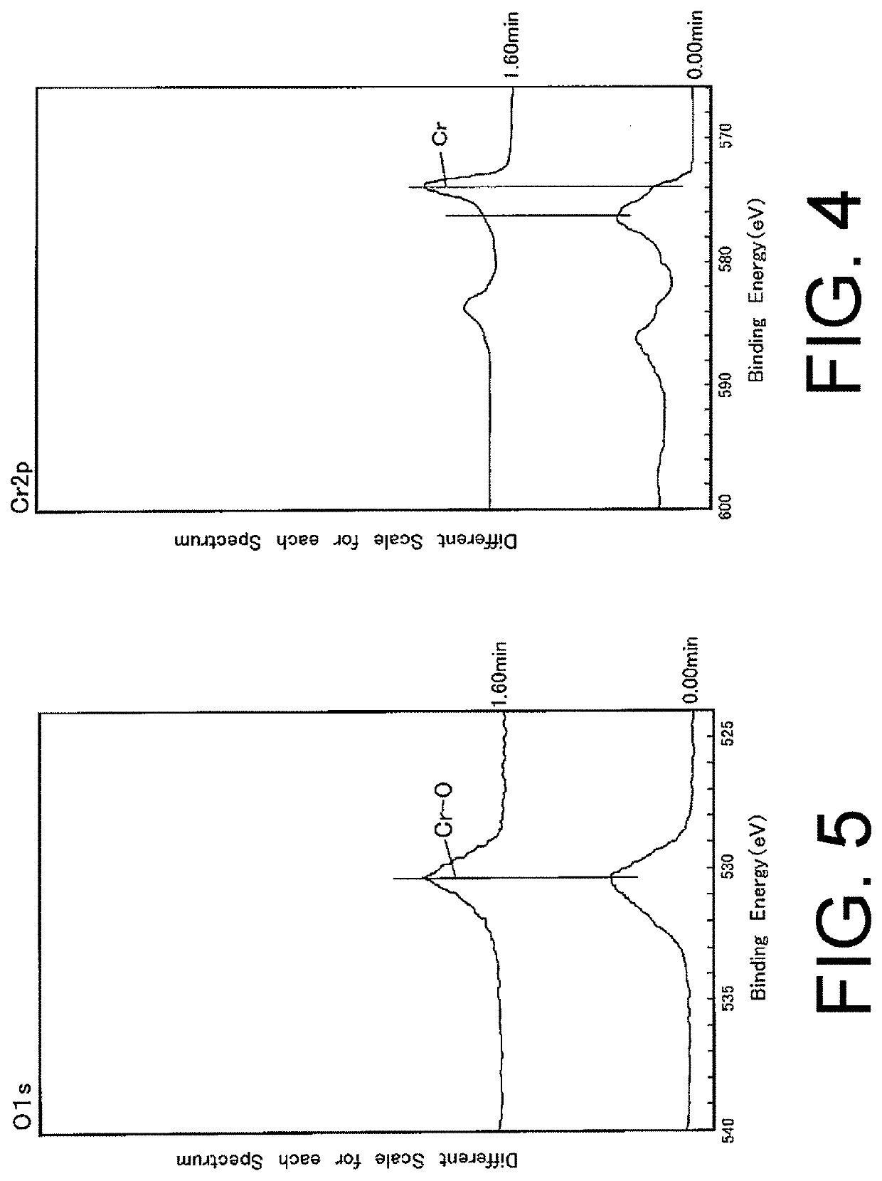
[0174]Only the hard mask film 3 in Example 2 was formed on another transparent substrate 1 and the hard mask film 3 was analyzed by X-ray photoelectron spectroscopy (with RBS co...


PUM

PropertyMeasurementUnit
binding energyaaaaaaaaaa
optical densityaaaaaaaaaa

Abstract

A light shielding film made up of a material containing one or more elements selected from silicon and tantalum and a hard mask film made up of a material containing chromium, oxygen, and carbon are laminated on a transparent substrate. The hard mask film is a single layer film having a composition gradient portion with increased oxygen content on the surface and on the neighboring region. The maximum peak for N1s in a narrow spectrum obtained via X-ray photoelectron spectroscopy analysis is the lower limit of detection or less. The portions excluding the composition gradient portion of the hard mask film have a 50 atom % or more chromium content, and the maximum peak for Cr2p in a narrow spectrum obtained via X-ray photoelectron spectroscopy analysis has a binding energy of 574 eV or less.

Description

CROSS REFERENCE TO RELATED APPLICATIONS[0001]This application is a National Stage of International Application No. PCT / JP2018 / 002072 filed Jan. 24, 2018, which claims priority to Japanese Patent Application No. 2017-034706 filed Feb. 27, 2017, and the contents of which is incorporated by reference in its entirety.TECHNICAL FIELD[0002]This disclosure relates to a mask blank, a method for manufacturing a transfer mask using the mask blank, and a method for manufacturing a semiconductor device using the transfer mask manufactured by the above-mentioned method. In particular, this disclosure relates to a mask blank to be suitably used in an exposure apparatus using, as an exposure light source, exposure light having a short wavelength of 200 nm or less, a method for manufacturing a transfer mask, and a method for manufacturing a semiconductor device.BACKGROUND ART[0003]Generally, in a manufacturing process of a semiconductor device, fine pattern formation is carried out using photolitho...

Claims


Application Information

Patent Timeline
Patent Type & Authority Patents(United States)
IPC IPC(8): G03F1/24H01L21/033
CPCG03F1/24H01L21/0332H01L21/0337G03F1/48G03F1/80G03F7/0002G03F7/0015
Inventor NOZAWA, OSAMUOHKUBO, RYOSHISHIDO, HIROAKI
Owner HOYA CORP
Why Eureka
Try Eureka