

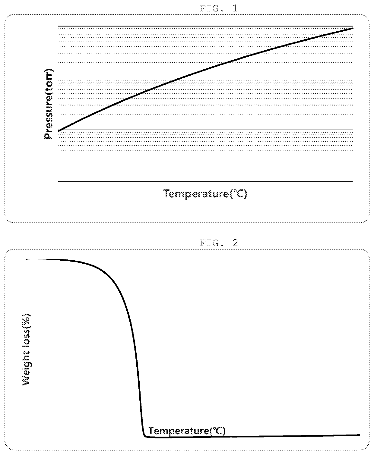
Composition for depositing silicon-containing thin film and method for producing silicon-containing thin film using the same
a technology of silicon-containing thin films and silicon precursors, which is applied in the direction of silicon compounds, organic chemistry, coatings, etc., can solve the problems of physical and electrical properties of thin films at the time of using existing silicon precursors, and achieve the effect of reducing the risk of aging
- Summary
- Abstract
- Description
- Claims
- Application Information
AI Technical Summary
Benefits of technology
Problems solved by technology
Method used
Image

Examples
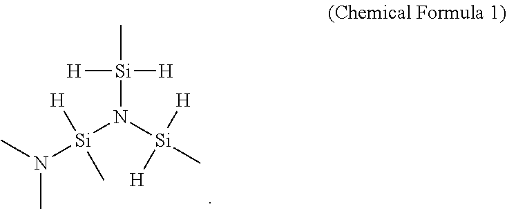
example 1
Preparation of Bis(Methylsilyl)Dimethylaminomethylsilyl Amine
Step 1: Preparation of bis(dimethylamino)methylsilyl amine
[0074]
[0075]500 g (3.1 mol) of hexamethyldisilazane (((CH3)3Si)2NH) was added to a flame-dried 2000 mL Schlenk flask under an anhydrous and inert atmosphere, 1,425 g (12.4 mol) of dichloromethylsilane ((CH3)Cl2SiH) was added slowly while maintaining a temperature to −25° C. and then the obtained reaction solution was slowly heated to 10° C. and stirred for 3 hours. Chlorotrimethylsilane ((CH3)3SiCl) produced in this mixed reaction solution and excessively added dichloromethylsilane ((CH3)Cl2SiH) were removed by simple distillation or distillation under reduced pressure. The recovered bis(chloromethylsilyl)amine ((SiHClCH3)2NH)) solution was stirred with pentane (n-Pentane), and 699 g (15.5 mol) of dimethylamine ((CH3)2NH) was slowly added while maintaining the temperature to −25° C. After the addition was completed, the reaction solution was slowly heated to room te...
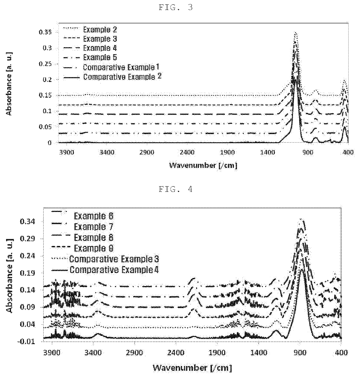
example 2
Production of Silicon Oxide Film by Plasma Enhanced Atomic Layer Deposition (PEALD) Using Bis(Methylsilyl)Dimethylamino Methylsilylamine
[0083]Film formation evaluation was conducted by using bis(methylsilyl)dimethylamino methylsilylamine prepared in Example 1 as the composition for forming a silicon oxide film in general plasma enhanced atomic layer deposition (PEALD) equipment using the known PEALD. As the reactive gas, oxygen was used together with plasma, and argon, which is an inert gas, was used for the purpose of purging. The film formation evaluation was conducted at 1.5 seconds for the reactive gas and plasma. The number of depositions was 270 cycles, and Table 1 shows a specific method for depositing a silicon oxide film.
[0084]A thickness of the deposited thin film was measured through an ellipsometer, the formation of the silicon oxide film was analyzed using an infrared spectrophotometer, and the composition of the silicon oxide film was analyzed using an X-ray photoelect...
example 3
Production of Silicon Oxide Film by Plasma Enhanced Atomic Layer Deposition (PEALD) Using Bis(Methylsilyl)Dimethylamino Methylsilylamine
[0085]Film formation evaluation was conducted by using bis(methylsilyl)dimethylamino methylsilylamine prepared in Example 1 as the composition for forming a silicon oxide film in general plasma enhanced atomic layer deposition (PEALD) equipment using the known PEALD. As the reactive gas, oxygen was used together with plasma, and argon, which is an inert gas, was used for the purpose of purging. The film formation evaluation was conducted at 1.5 seconds for the reactive gas and plasma. The number of depositions was 188 cycles, and Table 1 shows a specific method for depositing a silicon oxide film. In addition, FIG. 3 below shows analysis results of the film deposited using the infrared spectrometer.
PUM
| Property | Measurement | Unit |
|---|---|---|
| temperature | aaaaa | aaaaa |
| temperature | aaaaa | aaaaa |
| temperature | aaaaa | aaaaa |
Abstract
Description
Claims
Application Information