Method of etching an object, method of repairing pattern, nitride pattern and semiconductor device

Inactive Publication Date: 2003-03-11
KK TOSHIBA
View PDF12 Cites 27 Cited by
  • Summary
  • Abstract
  • Description
  • Claims
  • Application Information

AI Technical Summary

Benefits of technology

As summarized above, according to the invention, when the etching method by oxygen plasma using effects of H.sup.+ ions for etching a thin film having as its major component a nitrogen-containing compound layer of a metal such as chromium or nitrogen-containing compound semiconductor, etching takes place by chemical etching that produces highly volatile reaction products. Therefore, unlike the conventional etching methods using chlorine-group gases, the invention can suppress the micro-loading effect and can fabricate precise OPC (optical proximity repair) masks, Levenson phase shift masks, or and so on.
Additionally, according to the invention, a gas containing hydrogen and an oxygen gas can be used for etching instead of chloride gases heretofore used by the conventional dry etching methods, so it is a microstructure pattern fabrication method tha

Problems solved by technology

In the process of making microstructure patterns by dry etching, there is the problem that "micro-loading effect" occurs due to a difference in pattern density and degrades the uniformity of pattern sizes.
The "micro-loading effect" pertains to a phenomenon occurring upon simultaneously etching a pattern of a higher density and a pattern of a lower density: due to a difference in etching rate of a film from a location to another, the amount of reaction products by etching becomes locally dense or sparce, and convection of a large amount of reaction products by etching with a low volatility causes an un-uniformity in etching rate.
Heretofore, however, plasma etching techniques using the etching gas, containing Cl.sub.2 (chlorine) or F.sub.2 (fluorine) gases have been used in etching processes, and these techniques involve the problems that high-density plasma damages surfaces of devices and changes in composition ratio of Ga/N, etc. on surfaces.
Reaction products by etching of chromium (Cr)-group materials are usually low in volatility and are liable to cause the micro-loading effect in dry etching.
Therefore, it is an important issue how CD (critical dimension) controllability is enhanced in photomasks or reticles or in other circuit substrates.
As a result, the micro-loading effects is liable to occur, and it is extremely difficult for the mask to be CD controlled in the reticle plane.
If the CD controllability is poor, the resul

Method used


Image

  • Method of etching an object, method of repairing pattern, nitride pattern and semiconductor device
  • Method of etching an object, method of repairing pattern, nitride pattern and semiconductor device
  • Method of etching an object, method of repairing pattern, nitride pattern and semiconductor device

Examples


first embodiment

The first embodiment will be explained below in greater detail with reference to the first to fifth examples of the invention.

first example

(First Example)

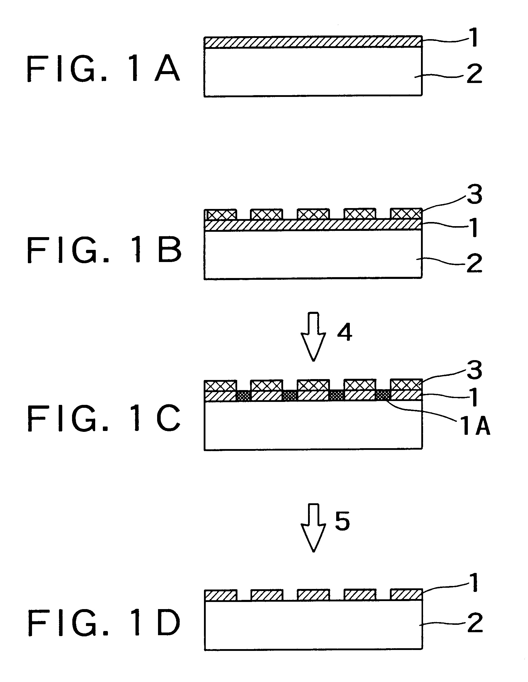
A photomask fabricating method using a chromium nitride (CrN.sub.x), taken as the first example of the invention, is first explained with reference to FIGS. 1A through 1D.

First referring to FIG. 1A, a chromium nitride film 1 was deposited on a substrate 2. More specifically, by introducing a cleaned 6.35 mm thick 6-inch quartz substrate 2 into a reactive sputtering apparatus, using Cr as the target material, the CrN.sub.x film 1 with 10 nm thickness as a opaque film, was deposited, using a mixed gas of a nitrogen / argon mixed gas under the pressure of 5 mTorr. After that, through ultrasonic cleaning, a mask blanks were obtained.

In case that a CrON film (not shown) as an anti-reflection film is to be formed on the CrN.sub.x film, the film is deposited in the same chamber, using a mixed gas of nitrous oxide (N.sub.2 O) and argon under to pressure of 5 mTorr such that the total thickness with the CrN.sub.x film 1 becomes 100 nm. Thereafter, through ultrasonic cleaning, a ...

second example

(Second Example)

Next explained is the second embodiment of the invention.

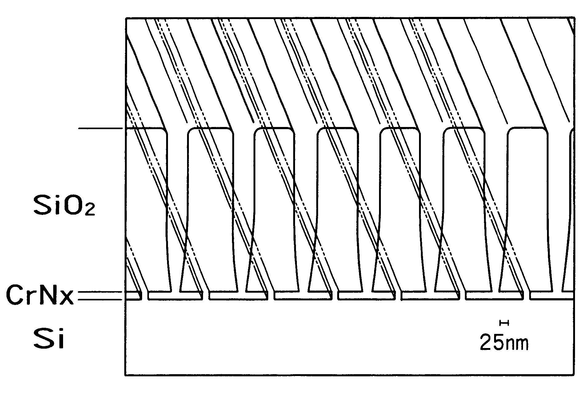
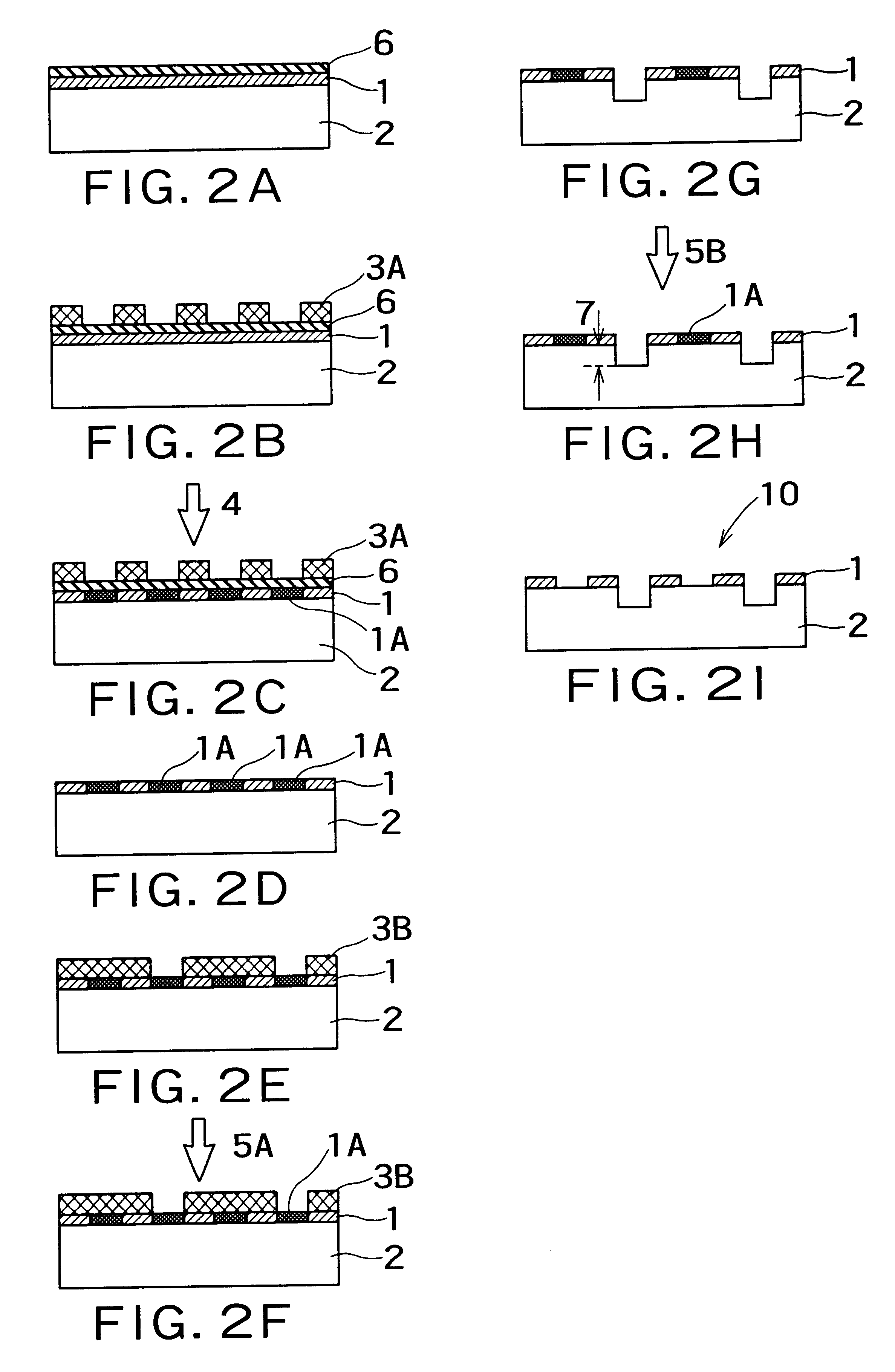
FIGS. 2A through 2I are cross-sectional views that show a manufacturing process according to the same embodiment. That is, these figures illustrate a manufacturing process for fabricating a single trench type Levenson phase shift mask according to the same.

First as shown in FIG. 2A, a chromium nitride layer 1 and a silicon oxide film 6 were deposited on a substrate 2. More specifically, by introducing a cleaned 6.35 mm thick 6-inch quartz substrate 2 into a reactive sputtering apparatus, using Cr as the target material, the CrN.sub.x film 1, 100 nm thick and functioning as a opaque film, was deposited, using an argon gas under the pressure of 5 mTorr. After that, through ultrasonic cleaning, a mask blanks were obtained. In case that a CrON film (not shown) as an anti-reflection film is to be formed on the CrN.sub.x film, the film is deposited in the same chamber, using a mixed gas of nitrous oxide (N.sub.2 O) a...


PUM

PropertyMeasurementUnit
Lengthaaaaaaaaaa
Lengthaaaaaaaaaa
Lengthaaaaaaaaaa

Abstract

A method of manufacturing a compound layer, containing a nitrified metal as a major component thereof and having a predetermined microstructure pattern, includes: an ion implantation step for implanting hydrogen ions into a predetermined region of a compound layer formed on a substrate to form an implanted region; and an etching step for selectively etching the implanted region by using a gas containing at least oxygen, to remove the implanted region of the compound layer while maintaining the other region as a microstructure pattern. By introducing a halogen element like fluorine in addition to hydrogen, fabrication of the pattern can be executed more reliably and more easily. As a result, volatility of reaction products produced upon etching the compound layer is enhanced, and micro-loading effects are suppressed. Thus, there are provided a method of fabricating a pattern of a compound layer capable of improving the CD controllability without using a dummy pattern, for example, and a compound layer having a microstructure pattern.

Description

BACKGROUND OF THE INVENTIONThis invention relates to a method of etching an object, a method of repairing a pattern, a nitride pattern and a semiconductor device, and more particularly to methods for making and repairing a microstructure pattern of a nitride film such as chromium nitride (CrN.sub.x) or gallium nitride (GaN) usable for manufacturing semiconductor devices or optical devices, and a nitride pattern obtained by any of those methods as well as a semiconductor device having such a nitride pattern.The invention is applicable to various fields such as masks suitable for use in exposure processes using various beams like optical or electrically charged beams or x-rays, or liquid crystal displays using those masks.A lot of nitrides including metallic nitrides or nitride semiconductors are materials that contribute to enhancing higher performances and higher functions of various devices such as electronic devices and optical devices, for example, importance of process technique...

Claims


Application Information

Patent Timeline
IPC IPC(8): C23C14/48G03F1/00H01L21/70H01L21/02H01L21/768H01L21/311H01L21/3065H01L33/00G03F1/20G03F1/22H01L21/027H01L21/302H01L33/32
CPCC23C14/48G03F1/72H01L21/3065H01L21/31116H01L21/7682H01L21/76865H01L21/76841H01L21/76807Y10T428/24926H01L21/76844H01L33/007H01L33/0075Y10T29/417
Inventor EZAKI, MIZUNORI
Owner KK TOSHIBA
Why Eureka
Try Eureka