Nitride compound semiconductor light emitting device and method for producing the same

a light-emitting device and compound semiconductor technology, which is applied in semiconductor devices, lasers, semiconductor lasers, etc., can solve the problems of high emission intensity, high nitrogen vacancy, and high defect concentration of nitride compound semiconductor crystals formed on conventional sapphire substrates

Inactive Publication Date: 2001-10-18
SHARP KK
View PDF7 Cites 126 Cited by
  • Summary
  • Abstract
  • Description
  • Claims
  • Application Information

AI Technical Summary

Problems solved by technology

It is known that the use of a quantum well layer having a thickness of about 10 nm or less for an active layer results in a high emission intensity.
Specifically, a nitride compound semiconductor crystal which has been formed on a conventional sapphire substrate has a high concentration of defects and/or nitrogen vacancies due to a lattice mismatch as high as 13% with the sapphire substrate.
In particular, a device which operates with a high current density, e.g., a laser device, is likely to be heated due to a high contact resistance, so that degradation may begin from an interface between the electrode and the p-type layer, leading to electrode destruction.
In addition, excessive heating might cause deterioration associated with the mobility of or increase in dislocations within the light emitting device, resulting in a decrease in the emission intensity or fluctuation in the emission wavelength.
Thus, the low hole density level in a p-type layer presently achievable under the conventional technique is detrimental to the emission characteristics and/or longevity of light emitting devices.
Moreover, a light emitting device formed on a conventional sapphire substrate not only suffers from the inactivation of Mg, but also receives unfavorable influences on an InGaN multiple quantum well activ

Method used


Image

  • Nitride compound semiconductor light emitting device and method for producing the same
  • Nitride compound semiconductor light emitting device and method for producing the same
  • Nitride compound semiconductor light emitting device and method for producing the same

Examples


example 3

[0083] (Example 3)

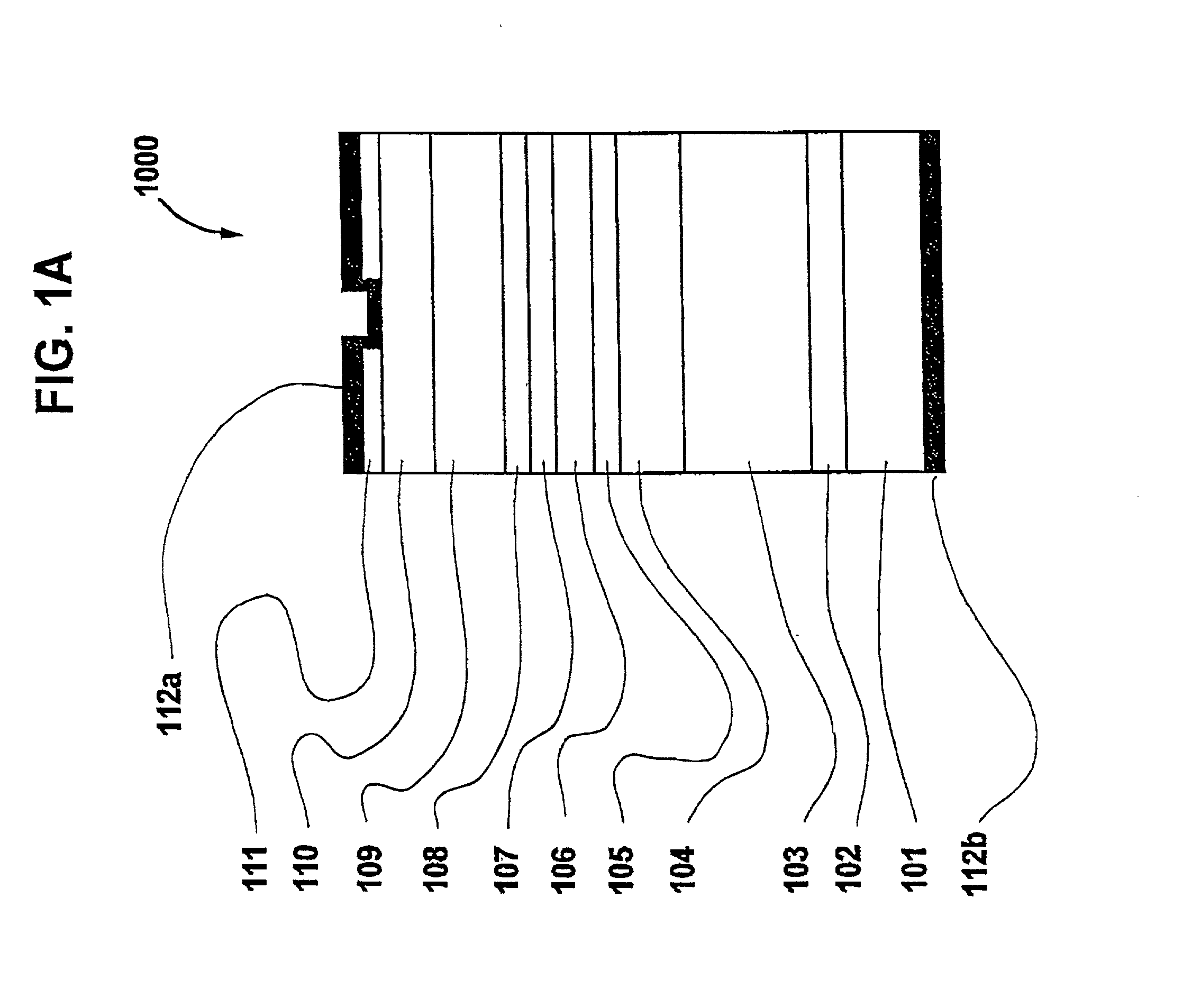
[0084] A semiconductor light emitting device 1000 was produced by a method similar to Example 2 while varying the thickness of the n-GaN layer 103, except that the growth temperature for the active layer 106 was fixed at about 750.degree. C. FIG. 10 shows results of a surface roughness plotting for the semiconductor light emitting device 1000 according to the present example with respect to the total thickness of the underlying layers between the substrate 101 and the active layer 106.

[0085] In FIG. 10, ".circle-solid." plots represent results obtained with a substrate tilt angle of 0.15.degree. in the direction from; ".largecircle." plots represent results obtained with a substrate tilt angle of 5.degree. in the direction; ".diamond-solid." plots represent results obtained with a substrate tilt angle of 1.7.degree. in the direction; and ".diamond." plots represent results obtained with a substrate tilt angle of 0.04.degree. in the direction. From FIG. 10, it c...

example 4

[0090] (Example 4)

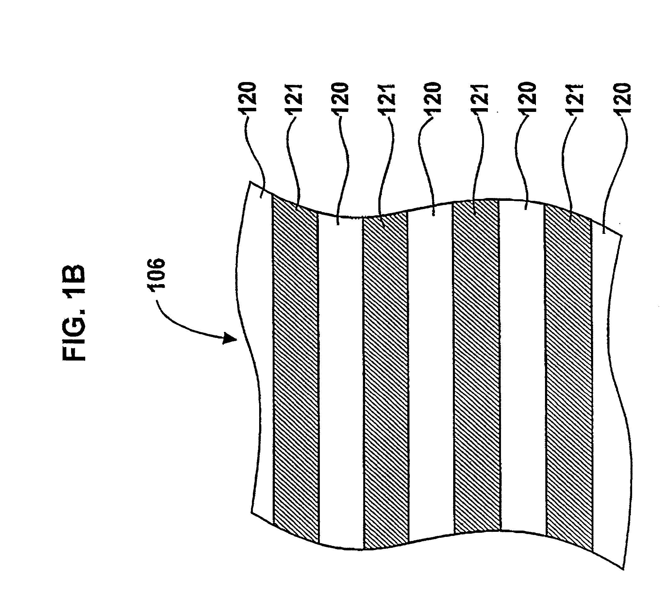
[0091] In Example 4 of the present invention, a semiconductor light emitting device 1000 in the form of an LED is produced, using the above-described growth wait period technique on a slightly-tilted substrate 101. In the present example, the relationship between the emission intensity when a current is injected to the resultant LED and the waiting time observed after growing each barrier layer 120 in the active layer 106 will be discussed.

[0092] By using a GaN substrate having a mirror-polished (0001) plane whose crystal orientation is actually tilted away from the direction by 0.15.degree. in the direction, a nitride compound semiconductor multilayer structure it grown in the manner shown in Example 1.

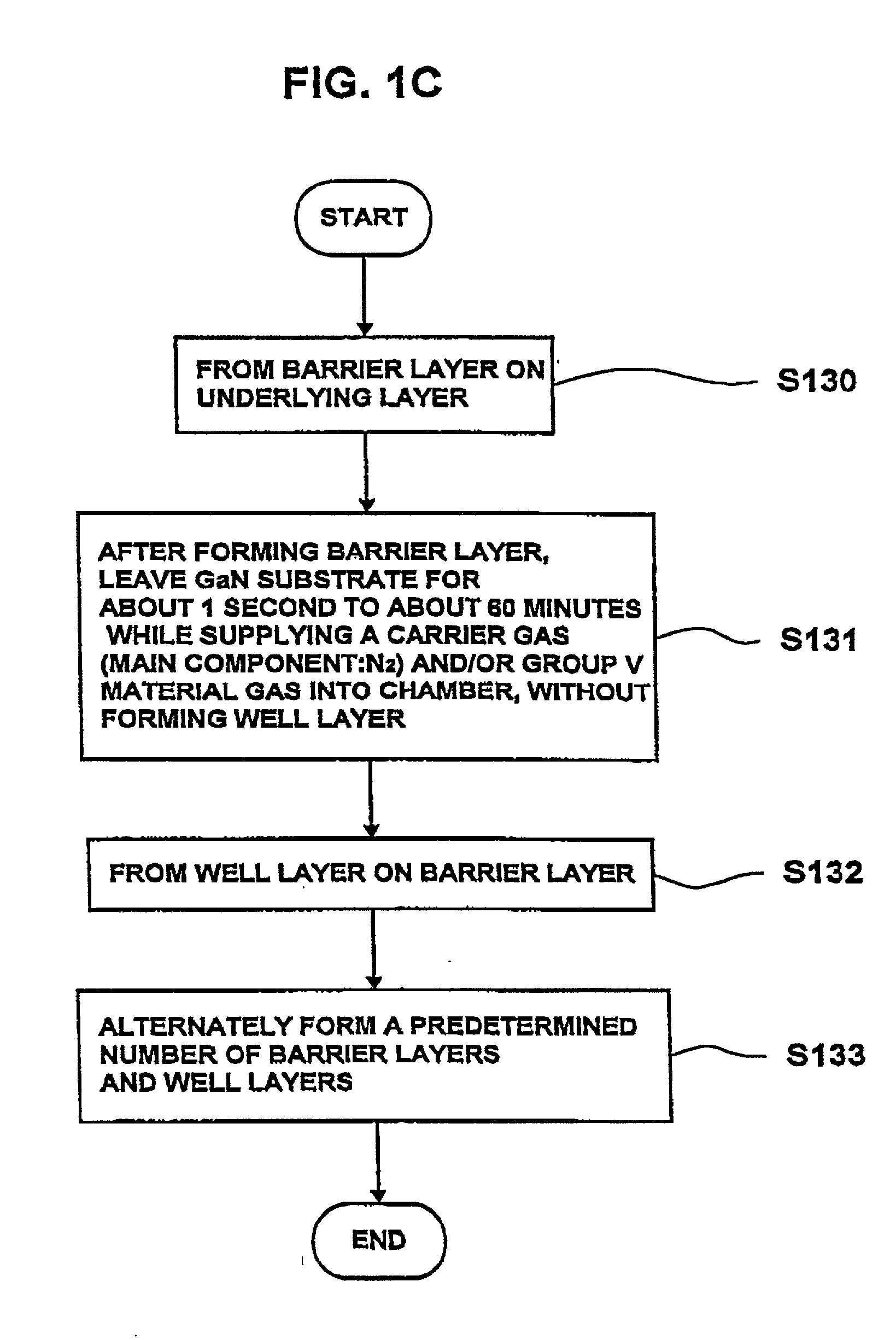
[0093] Now, steps for producing the active layer 106 according to the present example of the invention will be described with reference to a flow chart shown in FIG. 1C. After an n-GaN layer 103 is formed, growth conditions for the active layer 106 are adjusted so...

example 5

[0104] (Example 5)

[0105] In Example 5 of the present invention, a semiconductor light emitting device 1000 in the form of an LED is produced, using the above-described growth wait period technique on a GaN substrate having a mirror-polished (0001) plane whose crystal orientation is actually tilted away from the direction by 0.15.degree. in the direction. According to the present example, a predetermined wait period is observed after growing each barrier layer 120 within an active layer 106, and a predetermined wait period is observed after growing each well layer 121 within an active layer 106. In the present example, the relationship between the emission intensity when a current is injected to the resultant LED and the waiting time observed after growing each well layer 121 in the active layer 106 will be discussed. Thus, according to the present example, the step of leaving the substrate 101 for a predetermined waiting time (step S131) in the flowchart shown in FIG. 1C is perfor...


PUM


Abstract

A nitride compound semiconductor light emitting device includes: a GaN substrate having a crystal orientation which is tilted away from a <0001> direction by an angle which is equal to or greater than about 0.05° and which is equal to or less than about 2°, and a semiconductor multilayer structure formed on the GaN substrate, wherein the semiconductor multilayer structure includes: an acceptor doping layer containing a nitride compound semiconductor; and an active layer including a light emitting region.

Description

[0001] 1. Field of the Invention[0002] The present invention relates to a nitride compound semiconductor light emitting device formed on a GaN substrate, and a method for producing the same.[0003] 2. Description of the Related Art[0004] Conventionally, nitride compound semiconductor light emitting devices have been studied or utilized as light emitting devices or high power devices. In the case of light emitting devices, for example, light emitting devices covering a wide range of colors from blue to orange can be technically realized by using nitride compound semiconductors of various compositions. By taking advantage of such properties of nitride compound semiconductors, blue and green light emitting diodes (LEDs) have been realized in recent years. As for laser devices, blue-violet semiconductor laser devices are under development.[0005] By using a nitride compound semiconductor, a light emitting device is typically produced as follows. A current injection layer having n-type pro...

Claims


Application Information

Patent Timeline
IPC IPC(8): H01L33/06H01L33/16H01L33/32H01S5/30H01S5/32H01S5/323H01S5/343
CPCB82Y20/00H01L33/16H01L33/32H01S5/0207H01S5/2201H01S5/3054H01S5/3202H01S5/32341H01S5/34333H01S2304/04H01S2304/12H01S5/320275
Inventor UETA, YOSHIHIROYUASA, TAKAYUKIOGAWA, ATSUSHITSUDA, YUHZOHARAKI, MASAHIRO
Owner SHARP KK
Why Eureka
Try Eureka