Surface contamination analyzer for semiconductor wafers, method used therein and process for fabricating semiconductor device

a surface contamination analyzer and semiconductor wafer technology, applied in semiconductor/solid-state device testing/measurement, individual semiconductor device testing, instruments, etc., can solve the problems of reducing production yield, and affecting the quality of semiconductor devices

Inactive Publication Date: 2002-09-05
KK TOPCON
View PDF3 Cites 21 Cited by
  • Summary
  • Abstract
  • Description
  • Claims
  • Application Information

AI Technical Summary

Benefits of technology

[0015] It is another important object of the present invention to provide a process for fabricating a semiconductor device through which the production yield and reliability of semiconductor device are enhanced.

Problems solved by technology

If the surface of a semiconductor wafer is contaminated with trace elements, the miniature circuit components are much liable to be damaged, and the production yield is lowered.
The contamination due to the trace elements is serious in the process for fabricating the DRAMs.
In fact, the requirement for an ultra clean surface is getting severe and severe.
The organic compound particle is an obstacle in the removal of natural oxide.
Even though the manufacturer exposes the surface of the semiconductor wafer through the removal of the natural oxide before the deposition of metal, the organic compound particle does not allow the etchant to remove the natural oxide therebeneath.
Although the resistance in the direct contact between the metal layer and the semiconductor wafer is fallen within a target range, the contact resistance is locally increased, and uniform contact resistance is not achieved.
The organic contaminant particles are also obstacle against the ion-implantation, and do not allow the impurity region to have a target impurity profile.
While the semiconductor wafers are being exposed to the atmosphere, the molecular contaminants or contaminant clusters are unavoidably adhered to the surfaces of the semiconductor wafers.
However, the cleaning solution and / or the physical energy hardly reaches the contaminants in deep valleys or trenches and micro-holes formed in the three-dimensional structure.
If the contaminants are left on the bottom surfaces of the trenches and micro-holes, the residual contaminants vary the electric properties, and the circuit components formed in the trenches and micro-holes do not exhibit designed characteristics.
The defective circuit components are causative of reduction in production yield.
Even though the products pass the inspections, malfunction is liable to take place in the products, and, accordingly, those products are less reliable.
However, contaminants essentially composed of carbon-containing / nitrogen-containing molecules are hardly detected through the total reflection fluorescent x-ray spectroscopy.
Moreover, the mono-chromatic x-ray does not reach the bottom surfaces of extremely deep trenches, because the incident angle is small, and the contaminants on the bottom surfaces are not detectable.
A problem inherent is encountered in the first prior art surface contamination analysis technology in a small signal-to-noise ratio of the reflection from the trenches / holes with large aspect ratios.
On the other hand, a problem inherent in the second prior art surface contamination analyzer is a small signal-to-noise ratio of the vapor generated from an extremely narrow area.
However, the amount of contaminants vaporized from an extremely narrow area is too little to analyze it through the mass spectrometry.
Thus, the second prior art surface contamination analyzer is not available for a detailed report.
If the analysis on the surface contamination is inaccurate, it is difficult to optimize the cleaning against the contamination, and the residual contaminants are carried from an apparatus to another through the contaminated semiconductor wafer.
This results in reduction in production yield and poor reliability of semiconductor devices.
In metal, the secondary electrons are much liable to exceed the forbidden band, and lose the energy through the interaction with the electrons in the lattice.
However, the surfaces of the silicon wafers were damaged due to the ion-bombardment.
Micro-holes were formed in the silicon oxide layers, and the substrates were contaminated with the hydrocarbon compound.
However, the peripheral area was locally contaminated.
gle. Thus, the amount of current exhibited angle depend
If a contaminated semiconductor wafer is conveyed from one apparatus to another, the contaminants are also carried to the next stage, and the contamination is spread over the fabrication system.

Method used


Image

  • Surface contamination analyzer for semiconductor wafers, method used therein and process for fabricating semiconductor device
  • Surface contamination analyzer for semiconductor wafers, method used therein and process for fabricating semiconductor device
  • Surface contamination analyzer for semiconductor wafers, method used therein and process for fabricating semiconductor device

Examples


Embodiment Construction

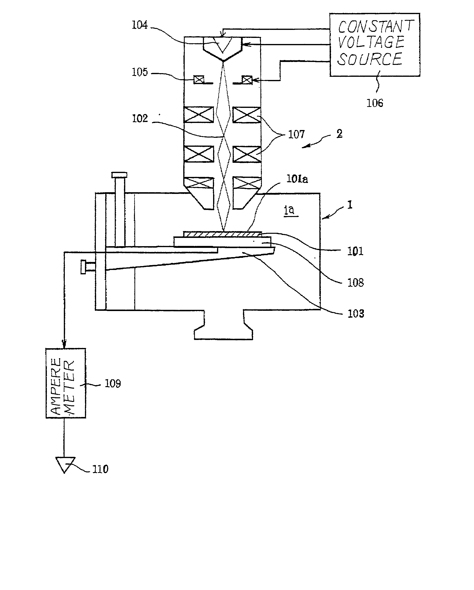
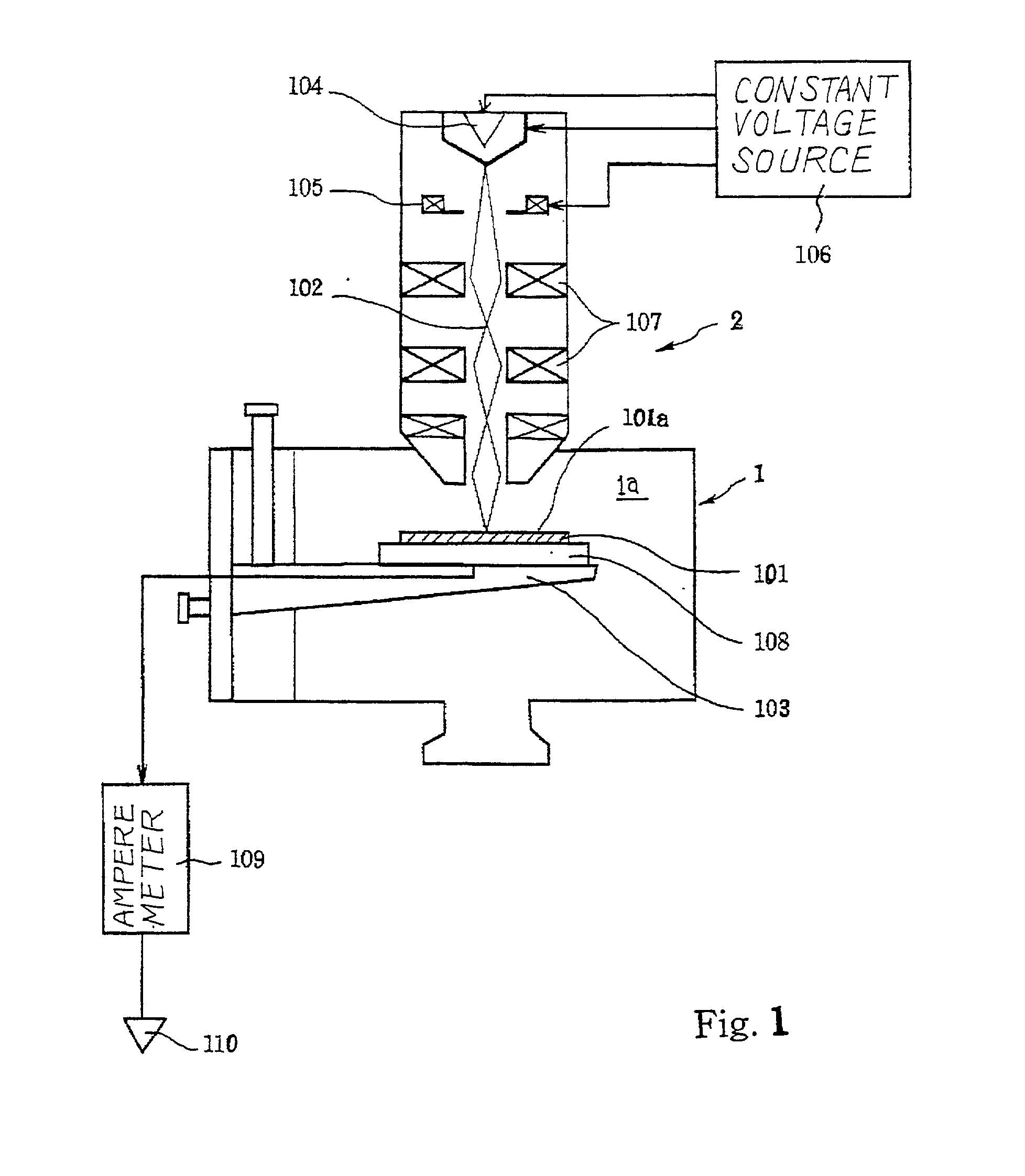
[0088] The inventors investigated the effects of the fabrication process containing the surface contamination analysis. The inventors prepared two 8-inch silicon wafers. Silicon oxide was thermally grown to 10 nanometers thick on the major surfaces of the silicon wafers, and, thereafter, the two silicon wafers were left in the clean room for a week. One of the silicon wafers, i.e. the first silicon wafer was assumed that the negative answer was given at step S12, and the other silicon wafer, i.e., the second silicon wafer was assumed that the positive answer was given at step S12.

[0089] The second silicon wafer was investigated at step S13. The surface contamination was serious, and the answer at step S14 was given affirmative. With the positive answer at step S14, the second silicon wafer was cleaned through a series of cleaning steps using water solution containing sulfuric acid and hydrogen peroxide, water solution containing ammonia and hydrogen peroxide and diluted hydrofluoric...


PUM

PropertyMeasurementUnit
acceleration energyaaaaaaaaaa
beam currentaaaaaaaaaa

Abstract

A semiconductor wafer is radiated with an electron beam so that the inelastic scattering takes place in the narrow region, and current flows out from the narrow region; the amount of current is dependent on the substance or substances in the narrow region so that the analyst evaluates the degree of contamination on the basis of the substance or substances specified in the narrow region.

Description

[0001] This invention relates to fabrication technologies for semiconductor devices and, more particularly, to a surface contamination analyzer for semiconductor wafers, a method used therein and a process for fabricating a semiconductor device.DESCRIPTION OF THE RELATED ART[0002] Semiconductor devices have been enhanced in integration density, and, accordingly, miniature circuit components are integrated on the small semiconductor chip. If the surface of a semiconductor wafer is contaminated with trace elements, the miniature circuit components are much liable to be damaged, and the production yield is lowered. Research and development efforts are being made on 1 giga-bit DRAM (Dynamic Random Access Memory). The contamination due to the trace elements is serious in the process for fabricating the DRAMs. Of course, miniaturization is the key technologies in the development. A cleaning technology is also important for the highly reliable ultra large scale integration devices. In fact...

Claims


Application Information

Patent Timeline
Patent Type & Authority Applications(United States)
IPC IPC(8): G01N21/95G01R1/06G01N27/00G01Q30/10G01Q60/40G01R31/302G21K7/00H01L21/304H01L21/306H01L21/66H01L29/94
CPCG01N21/9501G21K7/00H01L21/02063H01L22/12H01J2237/24507H01J2237/24571H01J2237/24592
Inventor USHIKI, TAKEOYAMADA, KEIZOITAGAKI, YOHSUKETSUJIDE, TOHRU
Owner KK TOPCON
Why Eureka
Try Eureka