Organic electroluminescent devices with organic layers deposited at elevated substrate temperatures

an electroluminescent device and organic technology, applied in the field of organic led, can solve the problems of difficult to synthesize a material having all the required properties, amorphous film, and presumably a large amount of defects, and achieve the effect of reducing device instability

Inactive Publication Date: 2002-12-05
CITYU RES
View PDF2 Cites 11 Cited by
  • Summary
  • Abstract
  • Description
  • Claims
  • Application Information

AI Technical Summary

Benefits of technology

[0008] It is another object of the present invention to provide a method to improve the performance of an organic LED by depositing organic thin films at elevated substrate temperatures.
[0014] The use of crystalline organic thin films in organic LEDs eliminates the amorphous-crystalline phase transformation upon operation or storage and thus increases the device stability. The hot substrate deposition at elevated temperatures either produces a crystallized organic film or generates an amorphous film having a better short range order. As a result, both electrical and optical characteristics of the organic LEDs can be improved significantly.
[0044] The organic EL devices of this invention can employ a cathode constructed of any metal having a work function lower than 4.0 eV, such as calcium and lithium. The cathode can also be formed through alloying a low work function metal with a high work function metal. A bilayer structure of Al / LiF can also been used to enhance electron injection.
[0045] In the prior art, the organic light-emitting structure 110 is constructed by sequential vapor deposition of the hole-transporting layer 112, the light-emitting layer 114, and the electron-transporting layer 116 at room temperature. Thus all the organic layers in organic LEDs are amorphous. In the present invention, at least one of the organic layers is fully crystallized or partly crystallized during deposition, thus reducing the device instability caused by the amorphous-crystalline phase transformation. The thickness of an individual organic layer largely depends on the materials used in organic LEDs and the requirements for potential applications, and it can be varied from 3 to 2,000 nm with a preferred range of 30 to 300 nm.

Problems solved by technology

However, the resulting films are generally amorphous and presumably contain a considerable amount of defects.
Long-term stability is one of the critical issues for the commercial applications of organic LEDs.
878), however, this makes it difficult to synthesize a material having all the required properties.

Method used


Image

  • Organic electroluminescent devices with organic layers deposited at elevated substrate temperatures
  • Organic electroluminescent devices with organic layers deposited at elevated substrate temperatures
  • Organic electroluminescent devices with organic layers deposited at elevated substrate temperatures

Examples


example 1

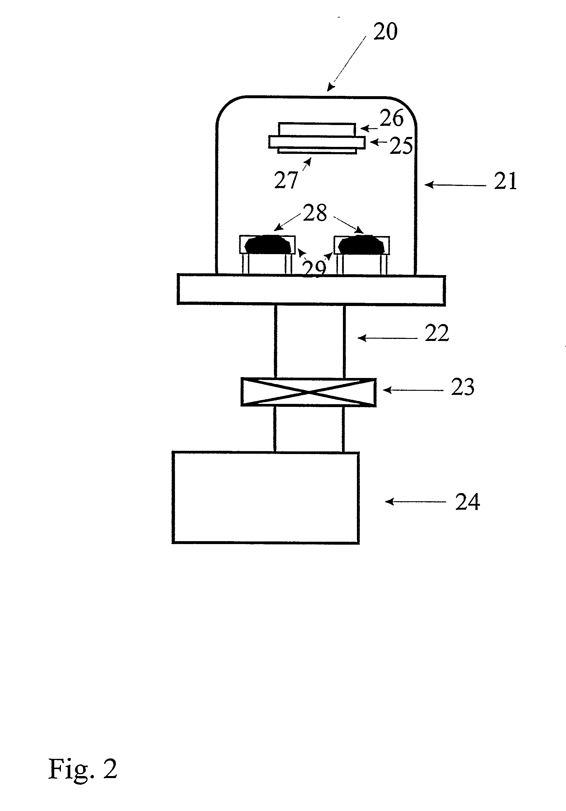
[0049] a) an ITO-coated glass was ultrasonicated sequentially in a commercial detergent, iso-propanol, ethanol, and methanol, rinsed in deionized water, and then dried in an oven. The substrate was further subjected to a UV-ozone treatment for 5-10 minutes.

[0050] b) the substrate was transferred into a deposition chamber from a loading chamber. Then the substrate was heated to 140.degree. C. and held at this temperature for more than 30 minutes before deposition.

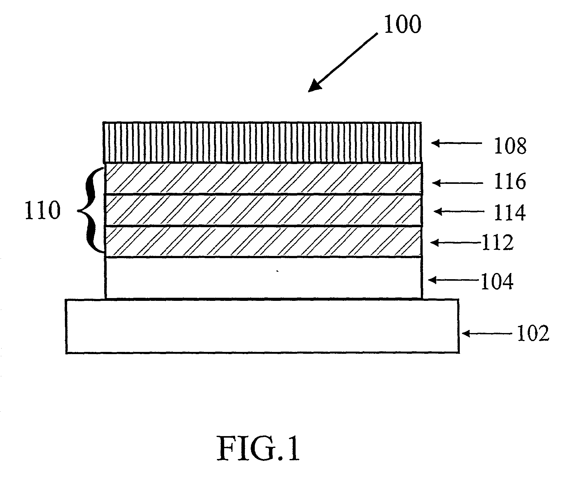
[0051] c) a 80 nm thick NPB hole-transporting layer was deposited on the ITO layer at 140.degree. C.;

[0052] d) a 60 nm thick Alq electron-transporting and light-emitting layer was deposited on the NPB layer at 140.degree. C.;

[0053] e) a 200 nm thick MgAg layer was deposited on the Alq layer by co-evaporation from two sources (Mg and Ag) at about 70.degree. C.

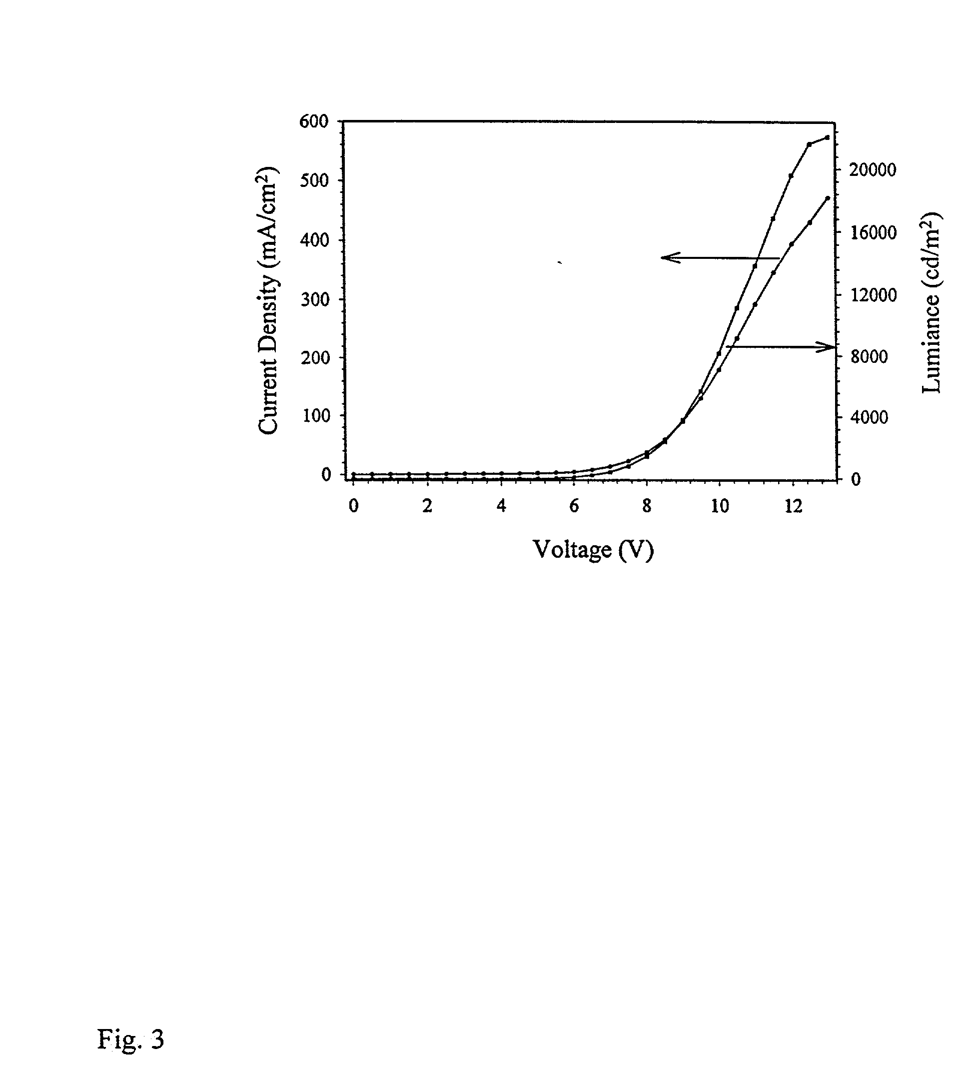
[0054] The electrical and optical properties of the device were characterized. The threshold voltage (defined as the voltage at which the device emits light with a lumin...

example 2 (

prior art)

[0055] a) an ITO-coated glass was ultrasonicated sequentially in a commercial detergent, iso-propanol, ethanol, and methanol, rinsed in deionized water, and then dried in an oven. The substrate was further subjected to a UV- ozone treatment for 5-10 minutes.

[0056] b) the substrate was transferred into a deposition chamber from a loading chamber, and held at room temperature during deposition.

[0057] c) a 80 nm thick NPB hole-transporting layer was deposited on the ITO layer at room temperature;

[0058] d) a 60 nm thick Alq electron-transporting and light-emitting layer was deposited on the NPB layer at room temperature;

[0059] e) a 200 mn thick MgAg layer was deposited on the Alq layer by co-evaporation from two sources (Mg and Ag) at about room temperature.

[0060] The electrical and optical properties of the device were characterized. The threshold voltage was determined to be 3.6 V. The luminance at a current density of 20 mA / cm.sup.2 was 618 cd / m.sup.2, and the efficiency wa...

example 3

[0061] a) an ITO-coated glass was ultrasonicated sequentially in a commercial detergent, iso-propanol, ethanol, and methanol, rinsed in deionized water, and then dried in an oven. The substrate was further subjected to a UV- ozone treatment for 5-10 minutes.

[0062] b) the substrate was transferred into a deposition chamber from a loading chamber. Then the substrate was heated to 140.degree. C. and held at this temperature for more than 30 minutes before deposition.

[0063] c) a 80 nm thick NPB hole-transporting layer was deposited on the ITO layer at 140.degree. C.;

[0064] d) a 60 nm thick Alq electron-transporting and light-emitting layer was deposited on the NPB layer at room temperature;

[0065] e) a 200 nm thick MgAg layer was deposited on the Alq layer by co-evaporation from two sources (Mg and Ag) at about room temperature.

[0066] The electrical and optical properties of the device were characterized. The threshold voltage was determined to be 4.0 V. The luminance at a current densit...


PUM

PropertyMeasurementUnit
work functionaaaaaaaaaa
temperatureaaaaaaaaaa

Abstract

An organic light-emitting diode has been disclosed, in which crystalline organic films were utilized to increase device stability upon operation. Correspondingly, a novel method has been developed to improve device performance through depositing organic electroluminescent materials at elevated substrate temperatures. The improvements are attributed to the formation of crystalline films or amorphous films with a better short range order.

Description

[0001] This invention relates to organic electroluminescent (EL) devices. More particularly, this invention relates to the use of organic crystalline flms deposited at elevated substrate temperatures for device fabrication.[0002] Since Tang and Vanslyke made the first multi-layer organic light-emitting diode by vacuum deposition of organic thin films at room temperature (see Appl. Phys. Lett. Vol. 51, 1987, P. 913), there has been considerable interest in the use of organic materials for fabrication of organic light-emitting diodes (LEDs). As a result, more and more new materials and processing technologies have been developed to improve the performance of the organic LEDs. Together with their wide viewing angle, high contrast, high brightness, and potentially low production cost, organic LEDs have a good potential for large-area flat panel display applications.[0003] In a basic organic LED structure, one organic layer is specifically chosen to inject and transport holes and the oth...

Claims


Application Information

Patent Timeline
Patent Type & Authority Applications(United States)
IPC IPC(8): C23C14/12C23C14/54H01L51/40H01L51/50H01L51/52
CPCC23C14/12H01L51/5012H01L51/001C23C14/541H10K71/164H10K50/11
Inventor LEE, SHUIT-TONGLEE, CHUN-SINGGAO, ZHI-QIANG
Owner CITYU RES
Why Eureka
Try Eureka