Semiconductor device

a semiconductor device and semiconductor technology, applied in semiconductor devices, diodes, electrical equipment, etc., can solve the problems of generating a large amount of heat, unable to place adjacent diodes, and foregoing conventional fluorescent lamp devices, etc., to achieve the effect of reducing the number of charges, improving the flexibility with which semiconductor devices are placed in equipment, and allowing the scaling down of equipmen

Inactive Publication Date: 2003-01-09
PANASONIC CORP
View PDF1 Cites 152 Cited by
  • Summary
  • Abstract
  • Description
  • Claims
  • Application Information

AI Technical Summary

Benefits of technology

0015] Since the high-performance active elements integrated in the compound semiconductor layer are obtainable, the semiconductor device can be placed at a desired site without using solder even if the semiconductor device is used at high temperature. This improves the flexibility with which the semiconductor device is placed in equipment and allows the scaling down of the equipment using the semiconductor device.
0016] Each of the plurality of active elements includes a MISFET having the first semicon

Problems solved by technology

However, the foregoing conventional fluorescent lamp device has the following problems.
However, the transistor, the diode, and the like cannot be positioned adjacent, e.g., a fluorescent lamp which generates a large amount of heat since the solder lacks durability at high temperatures.
As a result, the whole fluorescent lamp system is increased disadvantageously in size.
As a resul

Method used


Image

  • Semiconductor device
  • Semiconductor device
  • Semiconductor device

Examples


embodiment 1

[0042] Embodiment 1

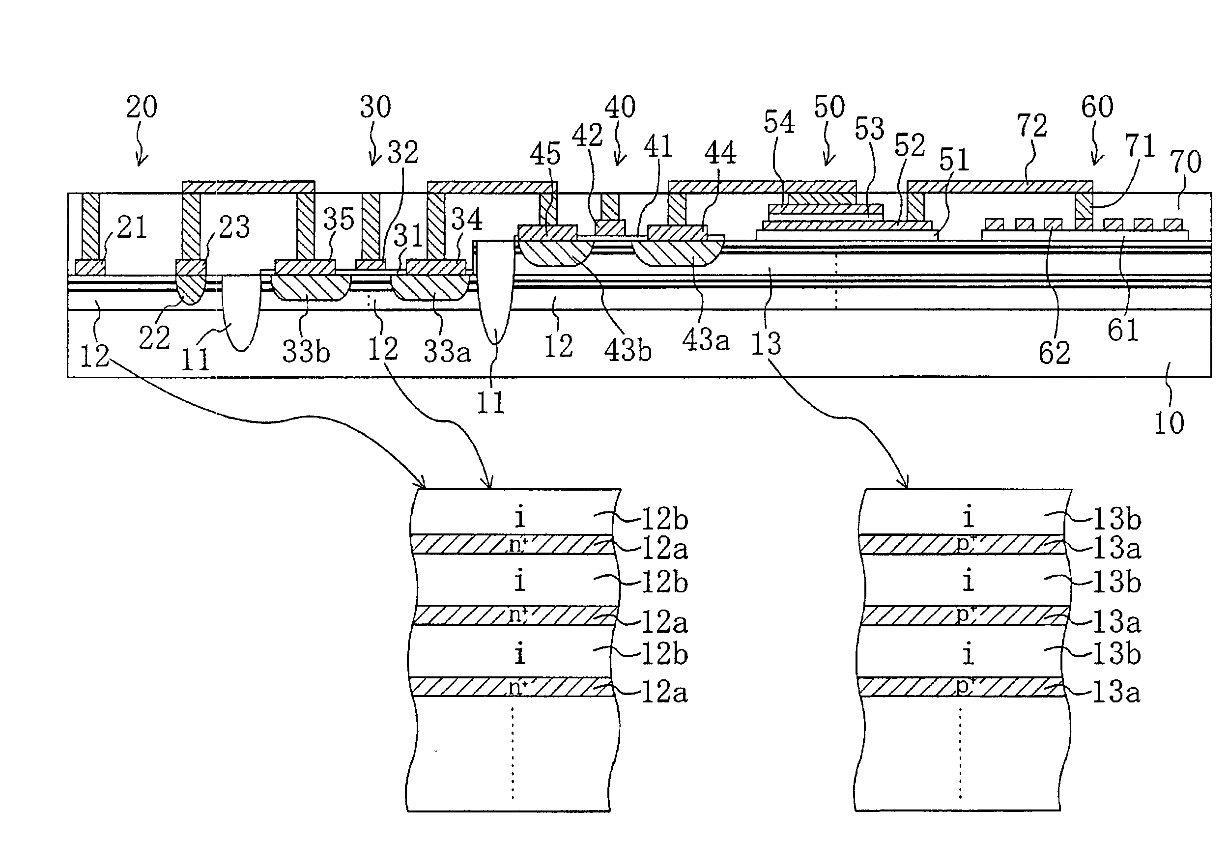
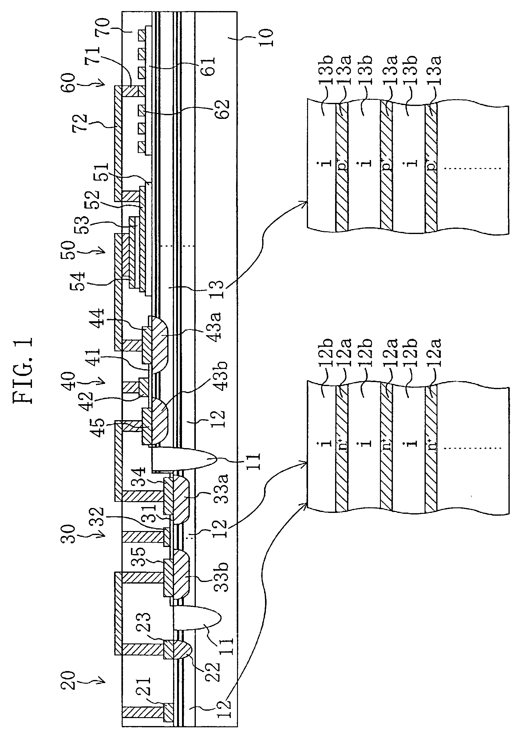
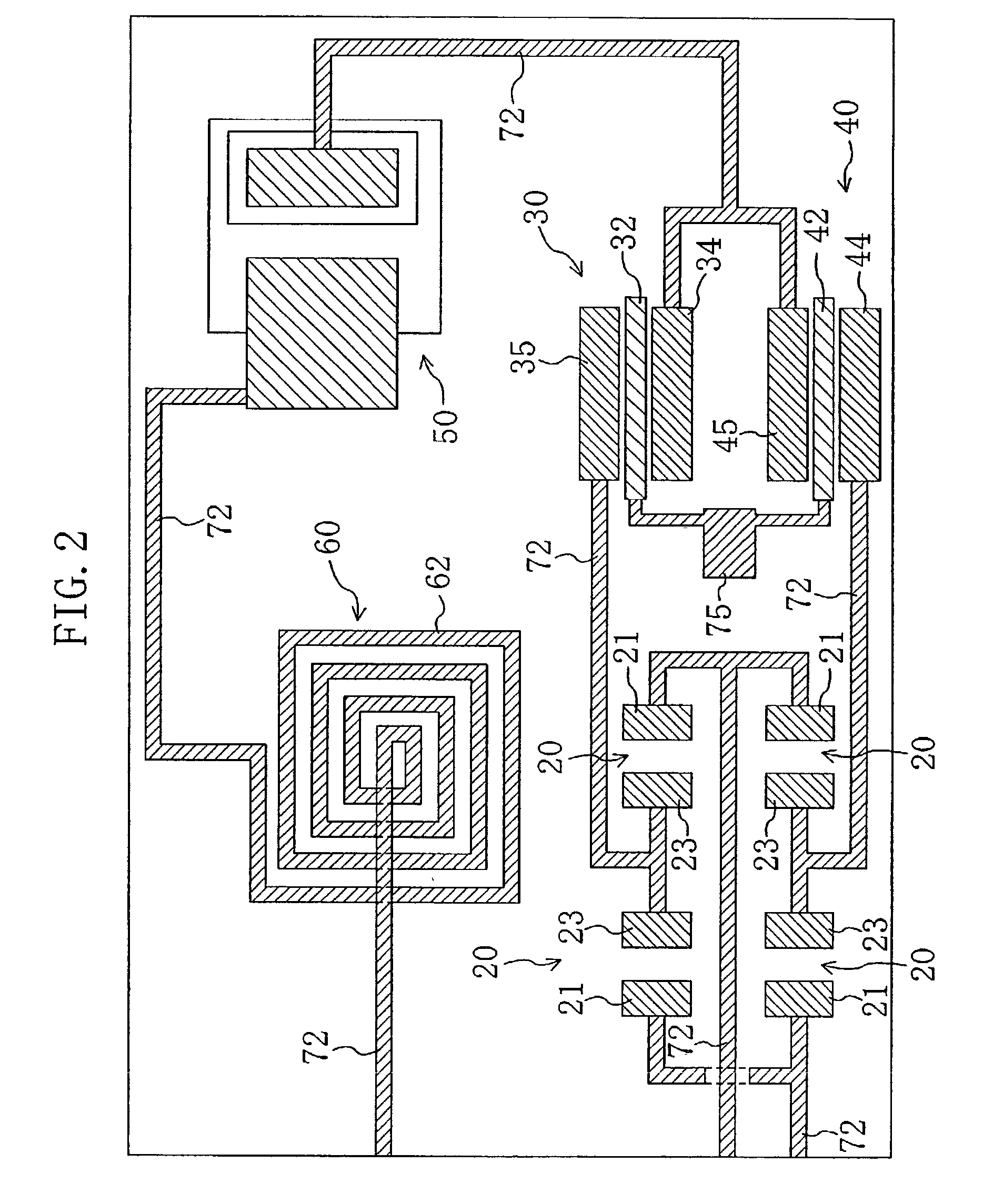
[0043] FIG. 1 is a cross-sectional view of an integrated semiconductor device composed of a Schottky diode, a MOSFET, a capacitor, and an inductor which are integrated in a SiC substrate according to a first embodiment of the present invention.

[0044] In a SiC substrate 10 which is a 4H--SiC substrate, an n-type first active region 12 doped with nitrogen at an average concentration of about 1.times.10.sup.17 atoms cm.sup.-3, a p-type second active region 13 doped with aluminum at an average concentration of about 1.times.10.sup.17 atoms cm.sup.-3 are provided upwardly in this order. The second active region 13 is partly removed such that the first active region 12 is partly exposed at the substrate. Insulation regions 11 each composed of a silicon dioxide film buried in a trench, which is for dividing the active regions 12 and 13 on a per element basis, are also provided in the SiC substrate 10.

[0045] As shown in the lower part of FIG. 1 under magnification, the fi...

embodiment 2

[0079] Embodiment 2

[0080] A description will be given next to a second embodiment of the present invention, which is an exemplary application of the semiconductor device described in the first embodiment to a lamp lighting circuit.

[0081] FIG. 6 is a cross-sectional view showing a structure of a fluorescent bulb lamp device 80 according to the present embodiment. As shown in the drawing, the fluorescent lamp device 80 comprises: a fluorescent lamp 81 composed of three luminescent tubes each having a generally U-shaped configuration which are coupled to each other; a lighting circuit 82 including such an element as a semiconductor chip for lighting the fluorescent lamp 81; a cover 83 for containing the lighting circuit 82; a mouth ring 84 attached to a tip of the cover 83; a globe 85 enveloping the fluorescent lamp 81; and a circuit board 86 for carrying the lighting circuit 82.

[0082] FIG. 7 is an electric circuit diagram showing a structure of the lighting circuit 82 in the fluoresce...

embodiment 3

[0103] Embodiment 3

[0104] In a third embodiment of the present invention, an ACCUFET (Accumulated Mode FET) using a multilayer structure composed of .delta.-doped layers and undoped layers to function as a large-current switching transistor will be used instead of the MOSFET of the integrated semiconductor device used in the first embodiment.

[0105] FIG. 15 is a cross-sectional view showing a structure of only the ACCUFET portion according to the present embodiment. As shown in the drawing, a lower active region 131 doped with aluminum at an average concentration of about 1.times.10.sup.17 atoms cm.sup.-3, an upper active region 132 formed on the lower active region 131 and doped with nitrogen at an average concentration of about 1.times.10.sup.17 atoms cm.sup.-3, n-type source and drain regions 133a and 133b formed by implanting nitrogen at a concentration of 1.times.10.sup.18 atoms cm.sup.-3 in the upper and lower active regions 132 and 131, respectively, a gate insulating film 134...


PUM


Abstract

In a SiC substrate (10), a first active region (12) composed of n-type heavily doped layers (12a) and undoped layers (12b), which are alternately stacked, and a second active region (13) composed of p-type heavily doped layers (13a) and undoped layers (13b), which are alternately stacked, are provided upwardly in this order. A Schottky diode (20) and a pMOSFET (30) are provided on the first active region (12). An nMOSFET (40), a capacitor (50), and an inductor (60) are provided on the second active region (13). The Schottky diode (20) and the MOSFETs (30, 40) have a breakdown voltage characteristic and a carrier flow characteristic due to a multilayer structure composed of delta-doped layers and undoped layers and are integrated in a common substrate.

Description

[0001] The present invention relates to a semiconductor power device for use in high-temperature applications requiring a high breakdown voltage and a large current, which is suited to high-power-consumption equipment such as a lighting device or an air conditioner.[0002] Silicon carbide (SiC) is a semiconductor having a band gap larger than that of silicon (Si) and therefore high dielectric resistance. Since silicon carbide retains stability at high temperatures, a semiconductor device formed by using a SiC substrate is expected to be applied to a next-generation power device or high-temperature operating device. In general, a power device is a generic name for a device which converts or controls high power and is termed a power diode, a power transistor, or the like. Exemplary applications of the power device include a transistor and a diode disposed in the inverter control unit of such equipment as a vacuum cleaner, a laundry washer, a refrigerator, a fluorescent lamp, or an air ...

Claims


Application Information

Patent Timeline
IPC IPC(8): H01L27/06H01L29/24H01L29/36H01L29/772H01L29/78H01L29/872
CPCH01L21/8213H01L21/8252H01L27/0629H01L27/0688H01L29/105H01L29/157H01L29/1608H01L29/365H01L29/7725H01L29/7838H01L29/812H01L29/872Y10S438/931Y10S438/957
Inventor YOKOGAWA, TOSHIYATAKAHASHI, KUNIMASAKITABATAKE, MAKOTOKUSUMOTO, OSAMUUENOYAMA, TAKESHIMIYAZAKI, KOJI
Owner PANASONIC CORP
Why Eureka
Try Eureka