Field emission devices using ion bombarded carbon nanotubes

a carbon nanotube and field emission technology, applied in the manufacture of discharge tube main electrodes, discharge tube/lamp manufacture, electrode systems, etc., can solve the problem of non-uniform current density between pixels, and achieve the effect of easy removal

Inactive Publication Date: 2003-03-06
HYPERION CATALYSIS INT
View PDF6 Cites 66 Cited by
  • Summary
  • Abstract
  • Description
  • Claims
  • Application Information

AI Technical Summary

Benefits of technology

0057] After the deposition of carbon nanotube particles by electrophoresis, low-temperature heating is performed to sustain the deposition of the carbon nanotubes on the cathodes and ensure easy removal of impurities which are incorporated into the field emitter during the deposition.

Problems solved by technology

The problem with metal emitter tips is that the control voltage required for emission is relatively high, e.g., around 100 V. Moreover, these emitter tips lack uniformity resulting in non-uniform current density between pixels.

Method used


Image

  • Field emission devices using ion bombarded carbon nanotubes
  • Field emission devices using ion bombarded carbon nanotubes
  • Field emission devices using ion bombarded carbon nanotubes

Examples


example ii

Emission Characteristics of Ion-Beam-Treated Nanotube Films

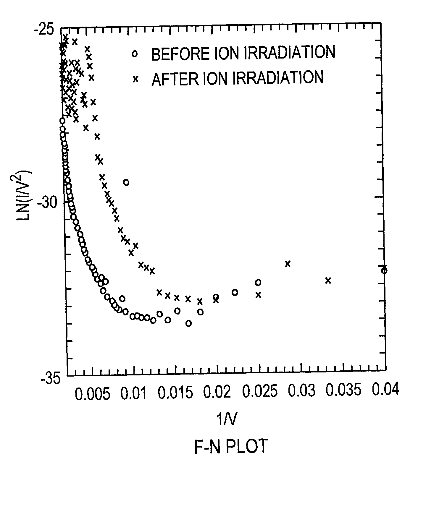
[0079] Carbon nanotube films fabricated by electrophoresis on an aluminum layer deposited on a glass have been locally irradiated with focused ion beams. A diode structure with a distance of 125 .mu.m between cathodes and anodes was used for emission measurement. A maximum emission current of 375 microamps with a turn-on voltage of 2.8 V / .mu.m for carbon nanotube emitters was found to decrease by focused ion beam irradiation to 1.1 V / .mu.m with increase in emission current by a factor of six.

[0080] The current range that was used in the test was in the low range with an anode voltage of about 400 to 500 volts, close to the turn-on (threshold) voltage for field emission. The change was from 0.05 to about 0.18 microamps to more than 0.9 microamps with a drastic change in the F-N plot shown in FIG. 9.

[0081] The physical and chemical effects of ion bombardment on carbon nanotubes are not entirely known. While not wishing to be b...


PUM

PropertyMeasurementUnit
lengthaaaaaaaaaa
lengthaaaaaaaaaa
diameteraaaaaaaaaa

Abstract

The present invention relates to a field emission device comprising an anode and a cathode, wherein said cathode includes carbon nanotubes which have been treated with an ion beam. The ion beam may be any ions, including gallium, hydrogen, helium, argon, carbon, oxygen, and xenon ions. The present invention also relates to a field emission cathode comprising carbon nanotubes, wherein the nanotubes have been treated with an ion beam. A method for treating the carbon nanotubes and for creating a field emission cathode is also disclosed. A field emission display device containing carbon nanotube which have been treated with an ion beam is further disclosed.

Description

[0001] This application claims the benefit of U.S. Provisional Application No. 60 / 298,228, filed Jun. 14, 2001, hereby incorporated by reference.[0002] The present invention relates to field emission cathodes which use carbon nanotubes.[0003] Field emission devices are devices that capitalize on the movement of electrons. A typical field emission device includes at least a cathode, emitter tips, and an anode spaced from the cathode. A voltage is applied between the cathode and the anode causing electrons to be emitted from the emitter tips. The electrons travel in the direction from the cathode to the anode.[0004] These devices can be used in a variety of applications including, but not limited to, microwave vacuum tube devices, power amplifiers, ion guns, high energy accelerators, free electron lasers, and electron microscopes, and in particular, flat panel displays. Flat panel displays can be used as replacements for conventional cathode ray tubes. Thus, they have application in t...

Claims


Application Information

Patent Timeline
Patent Type & Authority Applications(United States)
IPC IPC(8): H01J1/304H01J9/02
CPCB82Y10/00H01J1/304H01J9/025H01J31/127H01J2201/30469
Inventor TAKAI, MIKIO
Owner HYPERION CATALYSIS INT
Why Eureka
Try Eureka