Semiconductor light-emitting device and semiconductor light-emitting apparatus

a technology which is applied in the field of semiconductor light-emitting device and semiconductor light-emitting apparatus, can solve the problems of difficult to keep crystallinity at a high level, the inability to obtain good light-emitting characteristics, and the inability to form light-emitting elements in high precision, so as to improve the luminous efficiency, and improve the effect of crystallinity

Inactive Publication Date: 2003-06-12
SAMSUNG ELECTRONICS CO LTD
View PDF2 Cites 65 Cited by
  • Summary
  • Abstract
  • Description
  • Claims
  • Application Information

AI Technical Summary

Benefits of technology

0097] On the other hand, with the semiconductor light-emitting element (third semiconductor light-emitting element) of the invention which makes use of a different in composition or film thickness, the first conduction-type clad layer, active layer and second conduction-type clad layer are extended, for example, within the S plane formed by selective growth or within a plane parallel to a plane substantially equivalent to the S plane. The extension within the plane is readily feasible when crystal growth is continued during the formation of the S plane or the like. The crystal layer is shaped in the form of a substantially hexagonal pyramid or a substantially hexagonal pyramidal trapezoid. Where individual inclined planes are made of an S plane or the like, the emission region consisting of the first conduction-type clad layer, active layer and second conduction-type clad layer can be formed on all or part of the S planes. With a substantially hexagonal pyramidal trapezoid, the first conduction-type clad layer, active layer and second conduction-type clad layer can be formed on an upper surface parallel to the principal plane of the substrate. Since light is emitted by use of the inclined S planes, the light is attenuated owing to the multiple reflection for a parallel plate. Nevertheless, the inclined planes are advantageous in that the light does not undergo the influence of the multiple reflection and can come out of the semiconductor. The first conduction-type clad layer can be made of the same type of material with the same conduction type as the crystal layer constituting the S plane. After the formation of the crystal layer constituting the S plane, the clad layer can be continuously formed while controlling a concentration. In another instance, such a structure may be arranged that

Problems solved by technology

However, with such a semiconductor light-emitting element having such a structure as set out above, the fabrication process becomes complicated, so that the light-emitting element cannot be formed in high precision and because crystallinity is degraded, good light-emitting characteristics cannot be obtained.
In general, however, a substrate and a semiconductor layer may suffer degradation in crystallinity depending on the manner of dry etching, and especially,

Method used


Image

  • Semiconductor light-emitting device and semiconductor light-emitting apparatus
  • Semiconductor light-emitting device and semiconductor light-emitting apparatus
  • Semiconductor light-emitting device and semiconductor light-emitting apparatus

Examples


example 1

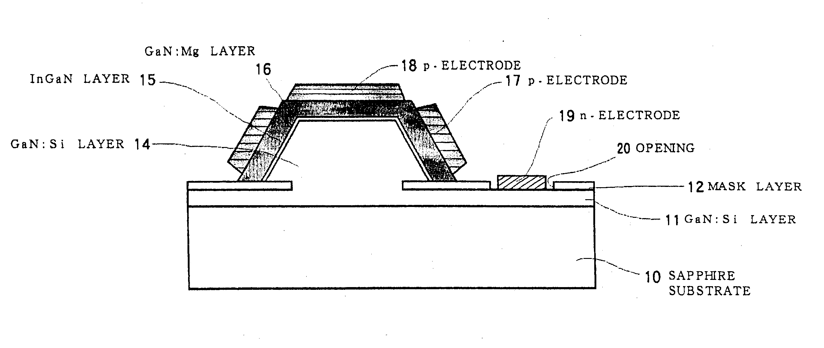
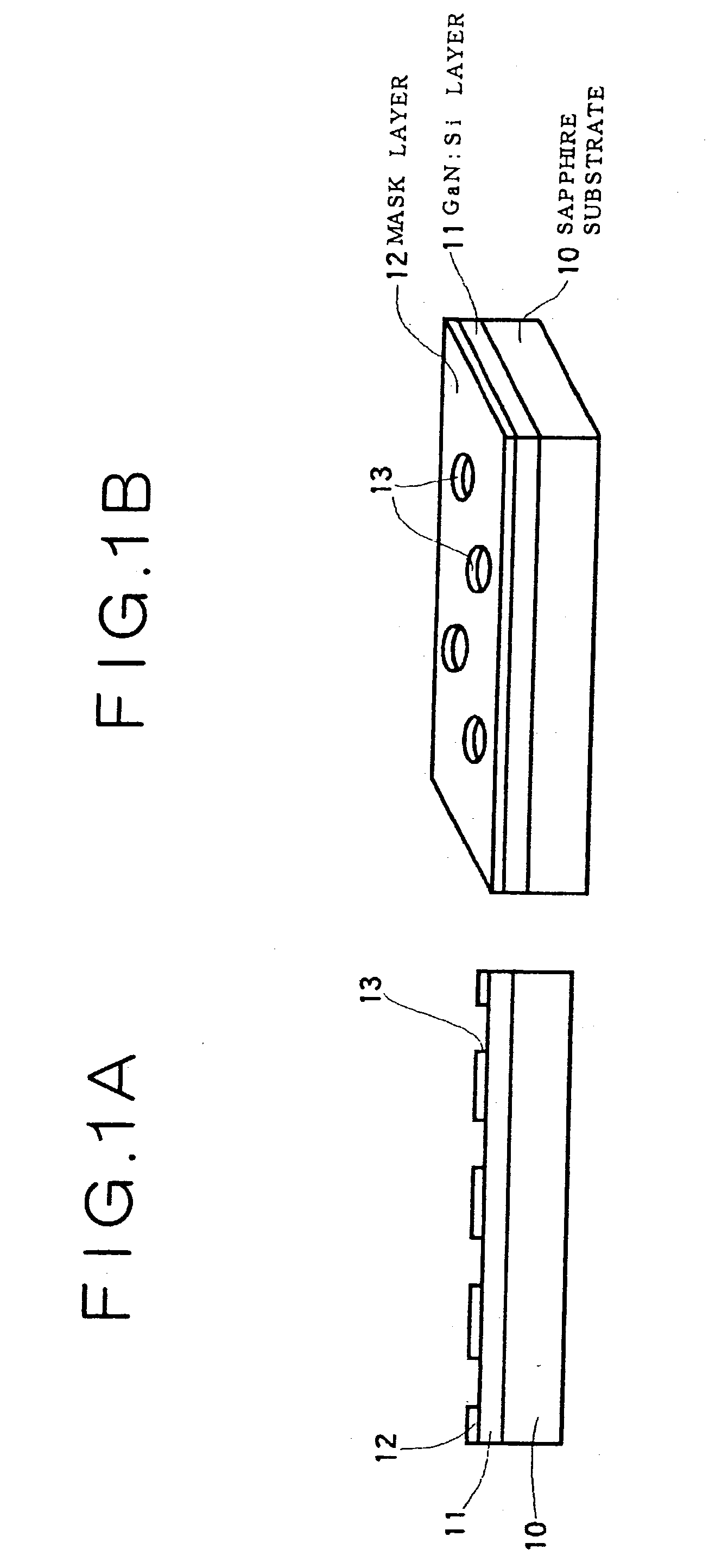
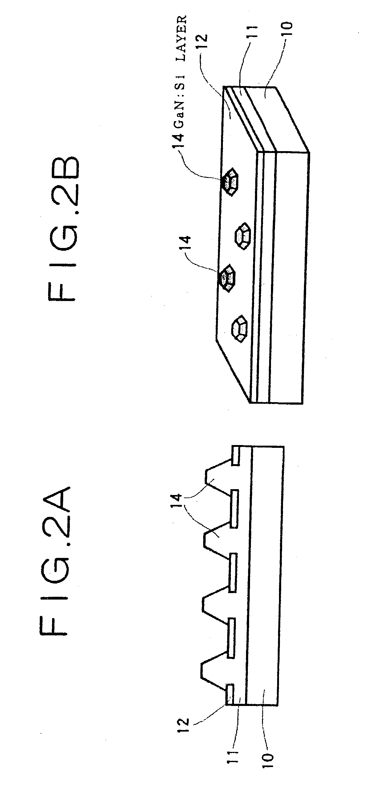
[0110] This example deals with direct selective growth on a sapphire substrate wherein a selective crystal growth layer having different crystal planes including an S plane and a C plane, and regions of the S plane and regions of the C plane are divided from each other and independent p-electrodes corresponding to two color light-emitting wavelengths are formed. With reference to FIGS. 1 to 6, an element structure is described along with a fabrication process thereof.

[0111] First, a low temperature buffer layer made of either AlN or GaN is formed on a sapphire substrate 10 having a C+ plane as a principal plane thereof at a low temperature of 500.degree. C. Thereafter, a mask layer 12 made of SiO.sub.2 or SiN is formed over the entire surface in a thickness ranging from 100 to 500 nm, and openings 13 with a size of approximately 10 .mu.m are formed according to photolithography by use of a hydrofluoric acid etchant (FIG. 1). In this example, the opening 13 is substantially in a roun...

example 2

[0121] This example is one which deals with direct selective growth on a sapphire substrate wherein a selective crystal growth layer having an S plane is formed and independent p-electrodes corresponding to two color light-emitting wavelengths are formed on the plane portion and the side portion of the S plane. Referring to FIGS. 7 to 12, the element structure is described along with its fabrication process.

[0122] First, a low temperature buffer layer made of either AlN or GaN is formed on a sapphire substrate 30 having a C+ plane as a substrate principal plane at a low temperature of 500.degree. C. After raising to a temperature of 1000.degree. C., a silicon-doped GaN layer 31 is formed. Subsequently, a mask layer 32 made of SiO.sub.2 or SiN is formed over the entire surface in a thickness ranging from 100 to 500 nm, and openings 33 with a size of approximately 10 .mu.m are formed according to photolithography using a hydrofluoric acid etchant (FIG. 7). In this example, the opening...

example 3

[0132] This example is one which deals with direct selective growth on a sapphire substrate wherein a selective crystal growth layer having an S plane is formed and independent p-electrodes corresponding to three color light-emitting wavelengths are formed. Referring to FIGS. 13 to 18, the element structure is described along with its fabrication process.

[0133] First, a low temperature buffer layer made of either AlN or GaN is formed on a sapphire substrate 50 having a C+ plane as a substrate principal plane thereof at a low temperature of 500.degree. C. After raising to a temperature of 1000.degree. C., a silicon-doped GaN layer 51 is formed. Subsequently, a mask layer 52 made of SiO.sub.2 or SiN is formed over the entire surface in a thickness ranging from 100 to 500 nm, and openings 53 with a size of approximately 10 .mu.m are formed according to photolithography using a hydrofluoric acid etchant (FIG. 13). In this example, the opening 53 is substantially in a round shape, and th...


PUM


Abstract

A semiconductor light-emitting element having a structure that does not complicate a fabrication process, can be formed in high precision and does not invite any degradation of crystallinity is provided. A light-emitting element is formed, which includes a selective crystal growth layer formed by selectively growing a compound semiconductor of a Wurtzite type, and a clad layer of a first conduction type, an active layer and a clad layer of a second conduction type, which are formed on the selective crystal growth layer wherein the active layer is formed so that the active layer extends in parallel to different crystal planes, the active layer is larger in size than a diffusion length of a constituent atom of a mixed crystal, or the active layer has a difference in at least one of a composition and a thickness thereof, thereby forming the active layer having a plurality of light-emitting wavelength region whose emission wavelengths differ from one another. The element is so arranged that an electric current or currents are chargeable into the plurality of light-emitting wavelength regions. Because of the structure based on the selective growth, it is realized that the band gap energy varies within the same active layer, thereby forming an element or device in high precision without complicating a fabrication process.

Description

[0001] This invention relates to a semiconductor light-emitting element making use of a compound semiconductor having a Wurtzite-type crystal structure and also to a semiconductor light-emitting device, an image display device and an illumination device, each using such a semiconductor light-emitting element making use of the compound semiconductor as mentioned above. More particularly, the invention relates to a semiconductor light-emitting element capable of emitting multi-color or white light by use of a compound semiconductor having a Wurtzite-type crystal structure and also to a semiconductor light-emitting device, an image display device and an illumination device.[0002] For a semiconductor light-emitting element, there is known an element which includes, entirely on a sapphire substrate, a builtup layer including a low temperature buffer layer, an n-type contact layer made of GaN doped with Si (silicon), an n-type clad layer made of Si-doped GaN formed on the contact layer, a...

Claims


Application Information

Patent Timeline
IPC IPC(8): H01L33/38H01L21/20H01L33/06H01L33/08H01L33/16H01L33/22H01L33/32
CPCH01L33/007H01L33/08H01L33/24H01L21/0237H01L21/0242H01L21/02639H01L21/0254H01L21/02576H01L21/02609H01L21/0262H01L21/02433H01L2224/48137
Inventor OKUYAMA, HIROYUKIDOI, MASATOBIWA, GOSHIOOHATA, TOYOHARU
Owner SAMSUNG ELECTRONICS CO LTD
Why Eureka
Try Eureka